LT1584/LT1585/LT1587
U
W U U
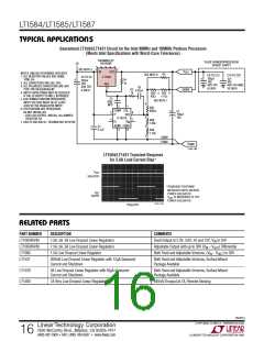
APPLICATIONS INFORMATION
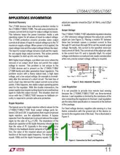
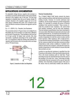
For adjustable voltage devices, negative side sensing is a
trueKelvinconnectionwiththebottomoftheoutputdivider
returned to the negative side of the load. The best load
regulation is obtained when the top of resistor divider R1
connects directly to the regulator output and not to the
load. Figure 5 illustrates this point. If R1 connects to the
load, the effective resistance between the regulator and the
load is:
Thermal Considerations
The LT1584/LT1585/LT1587 family protects the device
under overload conditions with internal power and thermal
limiting circuitry. However, for normal continuous load
conditions, do not exceed maximum junction temperature
ratings. It is important to consider all sources of thermal
resistance from junction-to-ambient. These sources in-
clude the junction-to-case resistance, the case-to-heat
sink interface resistance, and the heat sink resistance.
Thermal resistance specifications have been developed to
moreaccuratelyreflectdevicetemperatureandensuresafe
operating temperatures. The electrical characteristics sec-
tion provides a separate thermal resistance and maximum
junction temperature for both the control circuitry and the
power transistor. Older regulators, with a single junction-
to-case thermal resistance specification, use an average of
the two values provided here and allow excessive junction
temperatures under certain conditions of ambient tem-
perature and heat sink resistance. Calculate the maximum
junction temperature for both sections to ensure that both
thermal limits are met.
RP × (1 + R2/R1), RP = Parasitic Line Resistance
The connection shown in Figure 5 does not multiply RP by
the divider ratio. As an example, RP is about four milliohms
perfootwith16-gaugewire.Thistranslatesto4mVperfoot
at 1A load current. At higher load currents, this drop
represents a significant percentage of the overall regula-
tion. It is important to keep the positive lead between the
regulator and the load as short as possible and to use large
wire or PC board traces.
R
P
PARASITIC
LINE RESISTANCE
LT1584
ADJ
V
IN
IN
OUT
Junction-to-case thermal resistance is specified from the
IC junction to the bottom of the case directly below the die.
This is the lowest resistance path for heat flow. Proper
mounting ensures the best thermal flow from this area of
the package to the heat sink. Linear Technology strongly
recommends thermal compound at the case-to-heat sink
interface. Use a thermally conductive spacer if the case of
the device must be electrically isolated and include its
R1*
R2*
R
L
*CONNECT R1 TO CASE
CONNECT R2 TO LOAD
LT1584 • F05
Figure 5. Connection for Best Load Regulation
158457a
12

 Linear [ Linear ]