LT1584/LT1585/LT1587
U
W U U
APPLICATIONS INFORMATION
TheuseofcapacitorswithlowESR,lowESL,andgoodhigh
frequency characteristics is critical in meeting the output
voltage tolerances of these high speed microprocessors.
These requirements dictate a combination of high quality,
surface mount tantalum capacitors and ceramic capaci-
tors. The location of the decoupling network is critical to
transient response performance. Place the decoupling
networkascloseaspossibletotheprocessorpinsbecause
trace runsfromthe decouplingcapacitorstotheprocessor
pins are inductive. The ideal location for the decoupling
network is actually inside the microprocessor socket cav-
ity. In addition, use large power and ground plane areas to
minimize distribution drops.
put pin and the input pin or between the adjust pin and the
output pin to prevent die overstress.
On the adjustable LT1584/LT1585/LT1587, internal resis-
tors limit internal current paths on the adjust pin. There-
fore, even with bypass capacitors on the adjust pin, no
protection diode is needed to ensure device safety under
short-circuit conditions.
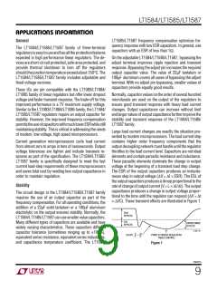
A protection diode between the input and output pins is
usuallynotneeded.Aninternaldiodebetweentheinputand
output pins on the LT1584/LT1585/LT1587 family can
handle microsecond surge currents of 50A to 100A. Even
with large value output capacitors it is difficult to obtain
those values of surge currents in normal operation. Only
with large values of output capacitance, such as 1000µF to
5000µF, and with the input pin instantaneously shorted to
ground can damage occur. A crowbar circuit at the input of
the LT1584/LT1585/LT1587 can generate those levels of
current, and a diode from output to input is then recom-
mended. This is shown in Figure 2. Usually, normal power
supply cycling or system “hot plugging and unplugging”
will not generate current large enough to do any damage.
Apossiblestabilityproblemthatoccursinmonolithiclinear
regulatorsiscurrentlimitoscillations.TheLT1585/LT1587
essentially have a flat current limit over the range of input
supply voltage. The lower current limit rating and 7V
maximum supply voltage rating for these devices permit
this characteristic. Current limit oscillations are typically
nonexistent, unless the input and output decoupling ca-
pacitors for the regulators are mounted several inches
from the terminals. The LT1584 differs from the LT1585/
LT1587 and provides current limit foldback as input-to-
output differential voltage increases. This safe-area char-
acteristic exhibits a negative impedance because increas-
ing voltage causes output current to decrease. Negative
resistance during current limit is not unique to the LT1584
devices and is present on many power IC regulators. The
valueofthenegativeresistanceisafunctionofhowfastthe
current limit is folded back as input-to-output voltage
increases. This negative resistance can react with capaci-
tors and inductors on the input and output to cause
oscillation during current limit. Depending on the values of
seriesresistances,theoverallsystemmayendupunstable.
However, the oscillation causes no problem and the IC
remainsprotected. Ingeneral, ifthisproblemoccursandis
unacceptable,increasingtheamountofoutputcapacitance
helps dampen the system.
The adjust pin can be driven on a transient basis ±7V with
respect to the output, without any device degradation. As
with any IC regulator, exceeding the maximum input-to-
outputvoltagedifferentialcausestheinternaltransistorsto
break down and none of the protection circuitry is then
functional.
D1
1N4002
(OPTIONAL)
LT1584-3.3
V
IN
OUT
V
OUT
IN
+
+
+
C1
C2
GND
10µF
22µF
D1
1N4002
(OPTIONAL)
LT1584
V
IN
OUT
V
OUT
IN
Protection Diodes
+
C1
10µF
C2
22µF
ADJ
R1
In normal operation, the LT1584/LT1585/LT1587 family
does not require any protection diodes. Older three-termi-
nal regulators require protection diodes between the out-
+
LT1584 • F02
R2
C
ADJ
Figure 2
158457a
10

 Linear [ Linear ]