LT1510/LT1510-5
W
U
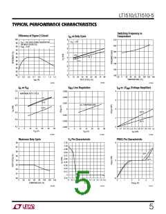
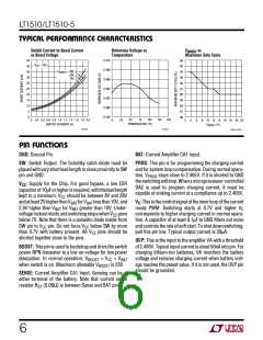
TYPICAL PERFORMANCE CHARACTERISTICS
Switch Current vs Boost Current
vs Boost Voltage
Reference Voltage vs
Temperature
VBOOST vs
Maximum Duty Cycle
50
45
40
35
30
25
20
15
10
5
2.470
2.468
2.466
2.464
2.462
2.460
2.458
96
95
94
93
92
91
90
89
88
87
86
V
CC
= 16V
V
= 38V
28V
18V
BOOST
0
0
0.2 0.4 0.6 0.8 1.0 1.2 1.4 1.6 1.8 2.0
0
50
75
100
125
150
25
2
4
6
8
10 12 14
22
16 18 20
TEMPERATURE (°C)
SWITCH CURRENT (A)
V
(V)
BOOST
1510 G07
1510 G14
LT1510 • TPC15
U
U
U
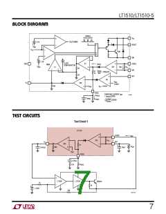
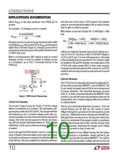
PIN FUNCTIONS
GND: Ground Pin.
BAT: Current Amplifier CA1 Input.
SW: Switch Output. The Schottky catch diode must be
placedwithveryshortleadlengthincloseproximitytoSW
pin and GND.
PROG: This pin is for programming the charging current
and for system loop compensation. During normal opera-
tion, VPROG stays close to 2.465V. If it is shorted to GND
theswitchingwillstop. Whenamicroprocessor-controlled
DAC is used to program charging current, it must be
capable of sinking current at a compliance up to 2.465V.
VCC: Supply for the Chip. For good bypass, a low ESR
capacitorof10µForhigherisrequired,withtheleadlength
kept to a minimum. VCC should be between 8V and 28V
andatleast2VhigherthanVBAT forVBAT lessthan10V,and
2.5V higher than VBAT for VBAT greater than 10V. Under-
voltage lockout starts and switching stops when VCC goes
below 7V. Note that there is a parasitic diode inside from
SW pin to VCC pin. Do not force VCC below SW by more
than 0.7V with battery present. All VCC pins should be
shorted together close to the pins.
VC:Thisisthecontrolsignaloftheinnerloopofthecurrent
mode PWM. Switching starts at 0.7V and higher VC
corresponds to higher charging current in normal opera-
tion. A capacitor of at least 0.1µF to GND filters out noise
and controls therate of soft start. To shut down switching,
pull this pin low. Typical output current is 30µA.
OVP: This is the input to the amplifier VA with a threshold
of2.465V. Typicalinputcurrentisabout50nAintopin. For
charging lithium-ion batteries, VA monitors the battery
voltage and reduces charging current when battery volt-
age reaches the preset value. If it is not used, the OVP pin
should be grounded.
BOOST: This pin is used to bootstrap and drive the switch
power NPN transistor to a low on-voltage for low power
dissipation. In normal operation, VBOOST = VCC + VBAT
when switch is on. Maximum allowable VBOOST is 55V.
SENSE: Current Amplifier CA1 Input. Sensing can be at
either terminal of the battery. Note that current sense
resistor RS1 (0.08Ω) is between Sense and BAT pins.
6

 Linear [ Linear ]