LT3587
APPLICATIONS INFORMATION
Board Layout Consideration
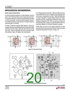
The voltage signals of the SW1, SW2 and SW3 pins have
riseandfalltimesofafewns. Minimizethelengthandarea
of all traces connected to the SW1, SW2 and SW3 pins
to reduce capacitive coupling between these fast nodes
and other circuitry. In particular, keep all the traces of the
As with all switching regulators, careful attention must be
paid to the PCB board layout and component placement.
To maximize efficiency, switch rise and fall times are made
as short as possible. To prevent electromagnetic interfer-
ence (EMI) problems, proper layout of the high frequency
switching path is essential.
feedback voltage pins (FB1, FB2, V and I ) away from
FB3
FB3
the switching node. Always use a ground plane under the
switching regulator to minimize interplane coupling.
In order to minimize magnetic field radiation, reduce the
parasiticinductancebykeepingthetracesthatconducthigh
switching currents short, wide and with minimal overall
loop area. These are typically the traces associated with
the switches. Figure 18 outlines the critical paths.
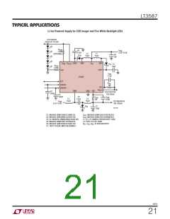
Finally, place as much of the output capacitors of each
channelclosetotheirrespectiveCAPpins.Recommended
component placement is shown in Figure 19.
C2
L2
L3
D
D
S3
S1
V
L1
L4
VIN
V
NEG
V
V
VIN
VIN
SW2
SW1
SW3
D
S2
CAP1
LT3587
GND
CAP3
LT3587
GND
C6
C7
LT3587
GND
Q2
C1
C4
C6
C6
Q1
Q3
3587 F18
Figure 18. High Current Paths
V
IN
CAP3
V
NEG
C6
(OPT)
C7
L4
C4
R
C
FB2
R
IFB3
V
OUT3
DS3
L3
FB2
C5
V
U1
C6
C3
IN
C2
R
FB1
DS2
DS1
C
FB1
L2
V
OUT1
L1
C1
C6
(OPT)
C6
(OPT)
3587 F19
V
CAP1
IN
Figure 19. Recommended Component Placement
3587fc
20

 Linear [ Linear ]