LTC3787
TYPICAL PERFORMANCE CHARACTERISTICS
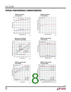
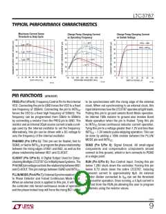
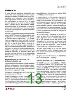
Maximum Current Sense
Threshold vs Duty Cycle
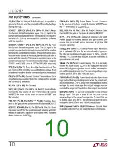
Charge Pump Charging Current
vs Operating Frequency
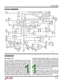
Charge Pump Charging Current
vs Switch Voltage
120
100
80
60
40
20
0
80
70
60
50
40
30
20
10
0
80
70
60
50
40
30
20
10
0
T = –60°C
FREQ = GND
I
= INTV
CC
LIM
FREQ = INTV
CC
T = –45°C
T = 25°C
I
= FLOAT
= GND
LIM
I
LIM
T = 130°C
T = 155°C
20 30 40 50 60
100
70 80 90
0
10
50 150 250 350 450 550 650 750
OPERATING FREQUENCY (kHz)
5
10
15
20
25
30
35
40
DUTY CYCLE (%)
SWITCH VOLTAGE (V)
3787 G26
3787 G27
3787 G25
PIN FUNCTIONS (QFN/SSOP)
FREQ (Pin ±/Pin 4): Frequency Control Pin for the Internal
to be synchronized with the rising edge of the external
clock. When not synchronizing to an external clock, this
input determines how the LTC3787 operates at light loads.
Pulling this pin to ground selects Burst Mode operation.
An internal 100k resistor to ground also invokes Burst
Mode operation when the pin is floated. Tying this pin
VCO. Connecting the pin to GND forces the VCO to a fixed
low frequency of 350kHz. Connecting the pin to INTV
CC
forces the VCO to a fixed high frequency of 535kHz. The
frequency can be programmed from 50kHz to 900kHz
by connecting a resistor from the FREQ pin to GND. The
resistor and an internal 20μA source current create a volt-
age used by the internal oscillator to set the frequency.
Alternatively, this pin can be driven with a DC voltage to
vary the frequency of the internal oscillator.
to INTV forces continuous inductor current operation.
CC
Tying this pin to a voltage greater than 1.2V and less than
INTV – 1.3V selects pulse-skipping operation. This can
CC
be done by adding a 100k resistor between the PLLIN/
MODE pin and INTV .
CC
PHASMD (Pin 2/Pin 5): This pin can be floated, tied to
SGND, ortiedtoINTV toprogramthephaserelationship
SGND (Pin 5/Pin 8): Signal Ground. All small-signal
components and compensation components should
connect to this ground, which in turn connects to PGND
at a single point.
CC
between the rising edges of BG1 and BG2, as well as the
phase relationship between BG1 and CLKOUT.
CLKOUT (Pin 3/Pin 6): A Digital Output Used for Daisy-
chainingMultipleLTC3787ICsinMultiphaseSystems.The
PHASMDpinvoltagecontrolstherelationshipbetweenBG1
RUN (Pin 6/Pin 9): Run Control Input. Forcing this pin
below 1.28V shuts down the controller. Forcing this pin
below 0.7V shuts down the entire LTC3787, reducing
quiescent current to approximately 8ꢀA. An external
and CLKOUT. This pin swings between SGND and INTV .
CC
PLLIN/MODE(Pin4/Pin7):ExternalSynchronizationInput
to Phase Detector and Forced Continuous Mode Input.
When an external clock is applied to this pin, it will force
the controller into forced continuous mode of operation
and the phase-locked loop will force the rising BG1 signal
resistor divider connected to V can set the threshold
IN
for converter operation. Once running, a 4.5ꢀA current is
sourced from the RUN pin allowing the user to program
hysteresis using the resistor values.
3787fc
9

 Linear Systems [ Linear Systems ]