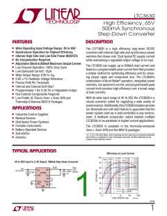
LTC3630
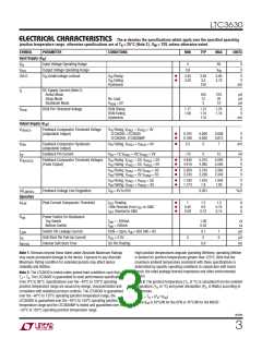
ELECTRICAL CHARACTERISTICS The l denotes the specifications which apply over the specified operating
junction temperature range, otherwise specifications are at TA = 25°C (Note 2). VIN = 12V, unless otherwise noted.
SYMBOL
PARAMETER
CONDITIONS
MIN
TYP
MAX
UNITS
Input Supply (V )
IN
V
V
Input Voltage Operating Range
Output Voltage Operating Range
4
65
V
V
IN
0.8
V
IN
OUT
l
l
UVLO
V
Undervoltage Lockout
V
V
Rising
Falling
3.45
3.30
3.65
3.5
150
3.85
3.70
V
V
mV
IN
IN
IN
Hysteresis
I
Q
DC Supply Current (Note 5)
Active Mode
165
12
5
270
20
10
ꢀA
ꢀA
ꢀA
Sleep Mode
No Load
RUN
Shutdown Mode
V
= 0V
V
RUN
RUN Pin Threshold Voltage
RUN Rising
RUN Falling
Hysteresis
1.17
1.06
1.21
1.10
110
1.25
1.14
V
V
mV
Output Supply (V
)
FB
V
Feedback Comparator Threshold Voltage
(Adjustable Output)
V
Rising, V
= V
PRG2
= 0V
= 0V
FB(ADJ)
FB
PRG1
l
l
LTC3630E, LTC3630I
0.792
0.788
0.800
0.800
0.808
0.812
V
V
LTC3630H, LTC3630MP
l
V
FBH
Feedback Comparator Hysteresis
(Adjustable Output)
V
V
Falling, V
= V
PRG2
2.5
5
7
mV
FB
PRG1
I
FB
Feedback Pin Current
= 1V, V
= 0V, V = 0V
PRG2
–10
0
10
nA
FB
PRG1
l
l
V
Feedback Comparator Threshold Voltages
(Fixed Output)
V
V
Rising, V
Falling, V
= SS, V
= SS, V
= 0V
= 0V
4.940
4.910
5.015
4.985
5.090
5.060
V
V
FB(FIXED)
FB
FB
PRG1
PRG1
PRG2
PRG2
l
l
V
FB
V
FB
Rising, V
Falling, V
= 0V, V
= 0V, V
= SS
= SS
3.260
3.240
3.310
3.290
3.360
3.340
V
V
PRG1
PRG1
PRG2
PRG2
l
l
V
FB
V
FB
Rising, V
Falling, V
= V
= V
= SS
= SS
1.780
1.770
1.810
1.8
1.840
1.83
V
V
PRG1
PRG1
PRG2
PRG2
Feedback Voltage Line Regulation
Peak Current Comparator Threshold
V
= 4V to 65V
0.001
%/V
ΔV
IN
LINEREG
Operation
l
l
l
I
I
Floating
1
0.45
0.09
1.2
0.6
0.12
1.4
0.75
0.15
A
A
A
PEAK
SET
100k Resistor from I to GND
SET
I
Shorted to GND
SET
R
Power Switch On-Resistance
Top Switch
Bottom Switch
ON
I
SW
I
SW
= –200mA
= 200mA
1.00
0.53
Ω
Ω
I
I
t
Switch Pin Leakage Current
Soft-Start Pin Pull-Up Current
Internal Soft-Start Time
RUN = Open, V = 65V, SW = 0V
0.1
5
1
6
μA
μA
ms
LSW
IN
V
SS
< 2.5V
3
SS
SS Pin Floating
0.8
INT(SS)
Note 1: Stresses beyond those listed under Absolute Maximum Ratings
may cause permanent damage to the device. Exposure to any Absolute
Maximum Rating condition for extended periods may affect device
reliability and lifetime.
High junction temperatures degrade operating lifetimes; operating lifetime
is derated for junction temperatures greater than 125°C. Note that the
maximum ambient temperature consistent with these specifications is
determined by specific operating conditions in conjunction with board
layout, the rated package thermal impedance and other environmental
factors.
Note 2: The LTC3630 is tested under pulsed load conditions such that
T ≈ T . The LTC3630E is guaranteed to meet performance specifications
J
A
from 0°C to 85°C. Specifications over the –40°C to 125°C operating
junction temperature range are assured by design, characterization and
correlation with statistical process controls. The LTC3630I is guaranteed
over the –40°C to 125°C operating junction temperature range, the
LTC3630H is guaranteed over the –40°C to 150°C operating junction
temperature range and the LTC3630MP is tested and guaranteed over the
–55°C to 150°C operating junction temperature range.
Note 3: The junction temperature (T , in °C) is calculated from the ambient
J
temperature (T , in °C) and power dissipation (P , in Watts) according to
A
D
the formula:
T = T + (P • θ )
JA
J
A
D
where θ is 43°C/W for the DFN or 45°C/W for the MSOP.
JA
3630fb
3

 Linear Systems [ Linear Systems ]