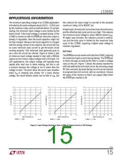
LT3592
APPLICATIONS INFORMATION
two poles in the loop. Rc provides a zero. With the recom-
terminal of the output capacitor C1). The SW and BOOST
nodes should be as small as possible. Finally, keep the
FB node small so that the ground pin and ground traces
will shield it from the SW and BOOST nodes. Include vias
near the exposed GND pad of the LT3592 to help remove
heat from the LT3592 to the ground plane.
mendedoutputcapacitor,theloopcrossoveroccursabove
theR C zero. Thissimplemodelworkswellaslongasthe
C C
valueoftheinductorisnottoohighandtheloopcrossover
frequency is much lower than the switching frequency.
With a larger ceramic capacitor that will have lower ESR,
crossover may be lower and a phase lead capacitor (C )
PL
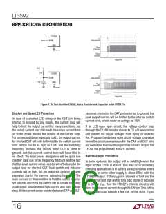
High Temperature Considerations
across the feedback divider may improve the transient
response. Large electrolytic capacitors may have an ESR
large enough to create an additional zero, and the phase
lead might not be necessary. If the output capacitor is
differentthantherecommendedcapacitor,stabilityshould
be checked across all operating conditions, including DIM
and BRIGHT current modes, voltage control via FB, input
voltage, and temperature.
The die temperature of the LT3592 must be lower than the
maximum rating of 125°C. This is generally not a concern
unless the ambient temperature is above 85°C. For higher
temperatures, extra care should be taken in the layout of
the circuit to ensure good heat sinking at the LT3592. The
maximum load current should be derated as the ambient
temperature approaches 125°C. The die temperature is
calculated by multiplying the LT3592 power dissipation
by the thermal resistance from junction to ambient.
Power dissipation within the LT3592 can be estimated
by calculating the total power loss from an efficiency
measurement and subtracting the catch diode loss. The
resultingtemperatureriseatfullloadisnearlyindependent
of input voltage. Thermal resistance depends upon the
layout of the circuit board, but 76°C/W is typical for the
3mm×2mmDFN(DDB10)package,and38°C/Wistypical
for the MS10E package.
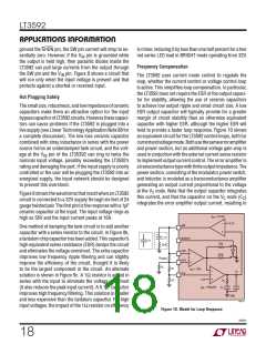
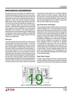
PCB Layout
ForproperoperationandminimumEMI,caremustbetaken
during printed circuit board layout. Figure 11 shows the
recommended component placement with trace, ground
plane,andvialocations.Notethatlarge,switchedcurrents
flowintheLT3592’sV andSWpins,thecatchdiode(D1),
IN
and the input capacitor (C2). The loop formed by these
components should be as small as possible and tied to
systemgroundinonlyoneplace.Thesecomponents,along
withtheinductorandoutputcapacitor,shouldbeplacedon
the same side of the circuit board, and their connections
shouldbemadeonthatlayer.Placealocal,unbrokenground
plane below these components, and tie this ground plane
to system ground at one location (ideally at the ground
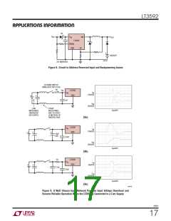
Higher Output Voltages
At higher output voltages, the choice of output capacitor
becomes especially critical. Many small case size ceramic
capacitorslosemuchoftheirratedcapacitancewellbelow
BRIGHT
SHDN
V
IN
SYS GND
3592 F11
Figure 11. A Good PCB Layout Ensures Proper, Low EMI Operation
3592fc
19

 Linear Systems [ Linear Systems ]