Specifications ispGDX160V/VA
Applications (Continued)
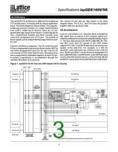
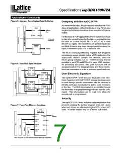
Figure 5. Address Demultiplex/Data Buffering
Designing with the ispGDXV/VA
As mentioned earlier, this architecture satisfies the PRSI
class of applications without restrictions: any I/O pin as a
single input or bidirectional can drive any other I/O pin as
output.
XCVR
I/OA
I/OB
Buffered
Data
OEA
OEB
ForthecaseofPDPapplications, thedesignerdoeshave
to take into consideration the limitations on pins that can
be used as control (MUX0, MUX1, OE, CLK) or data
(MUXA-D) inputs. The restrictions on control inputs are
not likely to cause any major design issues because the
input possibilities span 25% of the total pins.
To Memory/
Peripherals
Address
Latch
Address
D
Q
CLK
The MUXA-D input partitioning requires that designers
consciously assign pinouts so that MUX inputs are in the
appropriate, disjoint groups. For example, since the
MUXA group includes I/O0-39 (160 I/O device), it is not
possible to use I/O0 and I/O9 in the same MUX function.
As previously discussed, data path functions will be
assigned early in the design process and these restric-
tions are reasonable in order to optimize speed and cost.
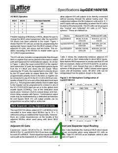
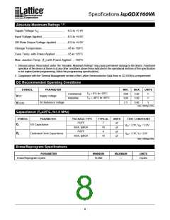
Figure 6. Data Bus Byte Swapper
XCVR
D0-7
D0-7
I/OA I/OB
XCVR
User Electronic Signature
OEA OEB
I/OA I/OB
The ispGDXV/VA Family includes dedicated User Elec-
tronic Signature (UES) E CMOS storage to allow users
OEA OEB
2
XCVR
to code design-specific information into the devices to
identify particular manufacturing dates, code revisions,
or the like. The UES information is accessible through
the boundary scan programming port via a specific com-
mand. This information can be read even when the
security cell is programmed.
D8-15
D8-15
I/OA I/OB
XCVR
OEA OEB
I/OA I/OB
OEA OEB
Security
The ispGDXV/VA Family includes a security feature that
prevents reading the device program once set. Even
when set, it does not inhibit reading the UES or device ID
code. It can be erased only via a device bulk erase.
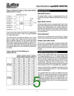
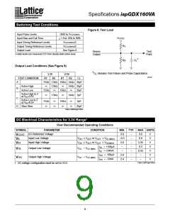
Figure 7. Four-Port Memory Interface
4-to-1
16-Bit MUX
Bidirectional
Port #1
Memory
To
Memory
OE1
Port
Port #2
OE2
OEM
Port #3
OE3
SEL0
SEL1
Port #4
OE4
Note: All OE and SEL lines driven by external arbiter logic (not shown).
7

 LATTICE [ LATTICE SEMICONDUCTOR ]