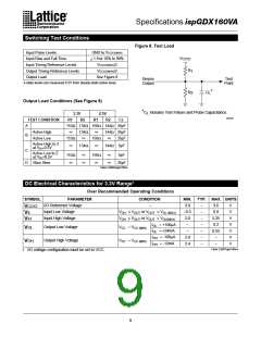
Specifications ispGDX160V/VA
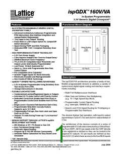
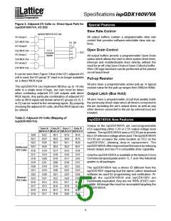
Figure 3. Adjacent I/O Cells vs. Direct Input Path for
ispGDX160V/VA, I/O D23
Special Features
Slew Rate Control
ispGDX160V/VA I/O Cell
I/O Group A
All output buffers contain a programmable slew rate
control that provides software-selectable slew rate op-
tions.
D21 MUX Out
S1 S0
I/O Group B
.m0
Open Drain Control
4 x 4
Crossbar
Switch
D22 MUX Out
I/O Group C
.m1
.m2
D23
All output buffers provide a programmable Open-Drain
option which allows the user to drive system level reset,
interrupt and enable/disable lines directly without the
needforanoff-chipOpen-DrainorOpen-Collectorbuffer.
Wire-OR logic functions can be performed at the printed
circuit board level.
.m3
D24 MUX Out
I/O Group D
D25 MUX Out
It can be seen from Figure 3 that if the D21 adjacent I/O
cell is used, the I/O group “A” input is no longer available
as a direct MUX input.
Pull-up Resistor
All pins have a programmable active pull-up. A typical
resistor value for the pull-up ranges from 50kΩ to 80kΩ.
The ispGDXV/VA can implement MUXes up to 16 bits
wide in a single level of logic, but care must be taken
when combining adjacent I/O cell outputs with direct
MUX inputs. Any particular combination of adjacent I/O
cells as MUX inputs will dictate what I/O groups (A, B, C
or D) can be routed to the remaining inputs. By properly
choosing the adjacent I/O cells, all of the MUX inputs can
be utilized.
Output Latch (Bus Hold)
All pins have a programmable circuit that weakly holds
the previously driven state when all drivers connected to
the pin (including the pin's output driver as well as any
other devices connected to the pin by external bus) are
tristated.
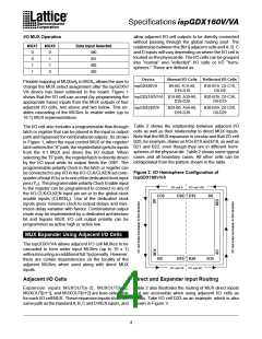
Table 2. Adjacent I/O Cells (Mapping of
ispGDX160V/VA)
ispGDX160VA New Features
Unique to the ispGDX160VA are user-programmable
I/Os supporting either 3.3V or 2.5V output voltage level
options. The ispGDX160VA uses a VCCIO pin to provide
the2.5Vreferencevoltagewhenused.TheispGDX160VA
VCCIO pin occupies the same location as VCC on the
ispGDX160V, allowing drop-in replacement. The
ispGDX160VAoffersimprovedperformancebyreducing
fanout delays and has PCI compatible drive capability.
Data A/ Data B/ Data C/ Data D/
MUXOUT MUXOUT MUXOUT MUXOUT
B20
B21
B22
B23
D16
D17
D18
D19
D20
D21
D22
D23
B16
B17
B18
B19
B22
B23
B24
B25
D18
D19
D20
D21
D18
D19
D20
D21
B14
B15
B16
B17
B21
B22
B23
B24
D17
D18
D19
D20
D19
D20
D21
D22
B15
B16
B17
B18
B19
B20
B21
B22
D15
D16
D17
D18
D21
D22
D23
D24
B17
B18
B19
B20
B18
B19
B20
B21
D14
D15
D16
D17
D22
D23
D24
D25
B18
B19
B20
B21
Reflected
I/O Cells
Only the ispGDX160VA is available in the fastest (3.5ns)
Commercial speed grade and in -5,-7, and -9ns Industrial
grades in all packages.
The ispGDX160VA has a device ID different from the
ispGDX160V requiring that the latest Lattice download
software be used for programming and verification. Al-
though the ispGDX160VA and ispGDX160V are
functionally equivalent, they are not 100% JEDEC com-
patible. All design files must be recompiled targeting the
ispGDX160VA.
Normal
I/O Cells
5

 LATTICE [ LATTICE SEMICONDUCTOR ]