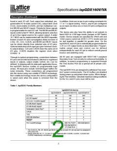
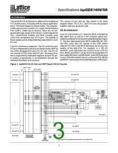
Specifications ispGDX160V/VA
Applications
The ispGDXV/VA Family architecture has been devel-
opedtodeliveranin-systemprogrammablesignalrouting
solution with high speed and high flexibility. The devices
are targeted for three similar but distinct classes of end-
system applications:
Programmable Switch Replacement (PSR)
Includes solid-state replacement and integration of me-
chanical DIP Switch and jumper functions. Through
in-system programming, pins of the ispGDXV/VA de-
vices can be driven to HIGH or LOW logic levels to
emulate the traditional device outputs. PSR functions do
not require any input pin connections.
Programmable, Random Signal
Interconnect (PRSI)
These applications actually require somewhat different
silicon features. PRSI functions require that the device
support arbitrary signal routing on-chip between any two
pins with no routing restrictions. The routing connections
are static (determined at programming time) and each
input-to-output path operates independently. As a result,
there is little need for dynamic signal controls (OE,
clocks, etc.). Because the ispGDXV/VA device will inter-
face with control logic outputs from other components
(such as ispLSI or ispMACH) on the board (which fre-
quently change late in the design process as control logic
is finalized), there must be no restrictions on pin-to-pin
signal routing for this type of application.
ThisclassincludesPCB-levelprogrammablesignalrout-
ing and may be used to provide arbitrary signal swapping
between chips. It opens up the possibilities of program-
mable system hardware. It is characterized by the need
to provide a large number of 1:1 pin connections which
are statically configured, i.e., the pin-to-pin paths do not
need to change dynamically in response to control in-
puts.
Programmable Data Path (PDP)
This application area includes system data path trans-
ceiver, MUX and latch functions. With today’s 32- and
64-bitmicroprocessorbuses,butstandarddatapathglue
components still relegated primarily to eight bits, PCBs
are frequently crammed with a dozen or more data path
glue chips that use valuable real estate. Many of these
applications consist of “on-board” bus and memory inter-
faces that do not require the very high drive of standard
glue functions but can benefit from higher integration.
Therefore, there is a need for a flexible means to inte-
gratetheseon-boarddatapathfunctionsinananalogous
way to programmable logic’s solution to control logic
integration. Lattice’s CPLDs make an ideal control logic
complement to the ispGDXV/VA in-system program-
mable data path devices as shown below.
PDP functions, on the other hand, require the ability to
dynamically switch signal routing (MUXing) as well as
latch and tri-state output signals. As a result, the pro-
grammableinterconnectisusedtodefinepossible signal
routes that are then selected dynamically by control
signals from an external MPU or control logic. These
functions are usually formulated early in the conceptual
design of a product. The data path requirements are
driven by the microprocessor, bus and memory architec-
ture defined for the system. This part of the design is the
earliest portion of the system design frozen, and will not
usually change late in the design because the result
would be total system and PCB redesign. As a result, the
ability to accommodate arbitrary any pin-to-any pin re-
routingisnotastrongrequirementaslongasthedesigner
has the ability to define his functions with a reasonable
degree of freedom initially.
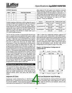
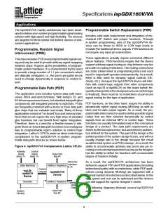
Figure 4. ispGDXV/VA Complements Lattice CPLDs
Address
Inputs
(from P)
Control
Inputs
(from P)
Data Path
Bus #1
ISP/JTAG
Interface
As a result, the ispGDXV/VA architecture has been
defined to support PSR and PRSI applications (including
bidirectional paths) with no restrictions, while PDP appli-
cations (using dynamic MUXing) are supported with a
minimalnumberofrestrictionsasdescribedbelow.Inthis
way, speed and cost can be optimized and the devices
can still support the system designer’s needs.
State Machines
Buffers / Registers
Control
Outputs
ispLSI/
ispMACH
Device
ispGDXV/VA
Device
Decoders
Buffers / Registers
Configuration
(Switch)
Outputs
The following diagrams illustrate several ispGDXV/VA
applications.
Data Path
Bus #2
System
Clock(s)
6

 LATTICE [ LATTICE SEMICONDUCTOR ]