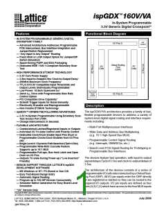
Specifications ispGDX160V/VA
I/O MUX Operation
allow adjacent I/O cell outputs to be directly connected
without passing through the global routing pool. The
relationship between the [N+i] adjacent cells and A, B, C
and D inputs will vary depending on where the I/O cell is
located on the physical die. The I/O cells can be grouped
into “normal” and “reflected” I/O cells or I/O “hemi-
spheres.” These are defined as:
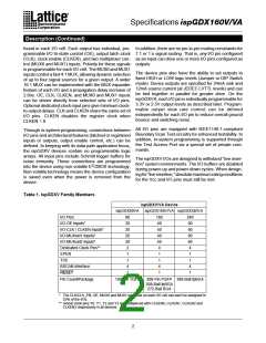
MUX1
MUX0
Data Input Selected
0
0
1
1
0
1
1
0
M0
M1
M2
M3
Device
Normal I/O Cells
Reflected I/O Cells
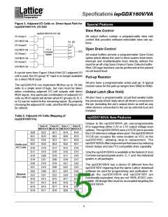
Flexible mapping of MUXsel to MUX allows the user to
x
x
ispGDX80VA
B9-B0, A19-A0,
D19-D10
B10-B19, C0-C19,
D0-D9
change the MUX select assignment after the ispGDXV/
VA device has been soldered to the board. Figure 1
shows that the I/O cell can accept (by programming the
appropriate fuses) inputs from the MUX outputs of four
adjacent I/O cells, two above and two below. This en-
ables cascading of the MUXes to enable wider (up to
16:1) MUX implementations.
ispGDX160V/VA B19-B0, A39-A0,
D39-D20
B20-B39, C0-C39,
D0-D19
ispGDX240VA
B29-B0, A59-A0,
D59-D30
B30-B59, C0-C59,
D0-D29
Table 2 shows the relationship between adjacent I/O
cells as well as their relationship to direct MUX inputs.
Note that the MUX expansion is circular and that I/O cell
B20, for example, draws on I/Os B19 and B18, as well as
B21 and B22, even though they are in different hemi-
spheres of the physical die. Table 2 shows some typical
cases and all boundary cases. All other cells can be
extrapolated from the pattern shown in the table.
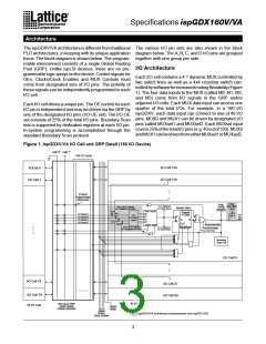
The I/O cell also includes a programmable flow-through
latch or register that can be placed in the input or output
path and bypassed for combinatorial outputs. As shown
in Figure 1, when the input control MUX of the register/
latch selects the “A” path, the register/latch gets its inputs
from the 4:1 MUX and drives the I/O output. When
selecting the “B” path, the register/latch is directly driven
by the I/O input while its output feeds the GRP. The
programmable polarity Clock to the latch or register can
be connected to any I/O in the I/O-CLK/CLKEN set (one-
quarter of total I/Os) or to one of the dedicated clock input
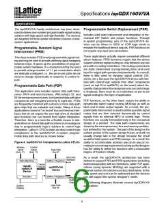
Figure 2. I/O Hemisphere Configuration of
ispGDX160V/VA
pins (Y ). The programmable polarity Clock Enable input
to the register can be programmed to connect to any of
the I/O-CLK/CLKEN input pin set or to the global clock
x
I/O cell 0
I/O cell 159
D39
D20 D19
D0
enable inputs (CLKEN ). Use of the dedicated clock
x
inputs gives minimum clock-to-output delays and mini-
mizes delay variation with fanout. Combinatorial output
mode may be implemented by a dedicated architecture
bit and bypass MUX. I/O cell output polarity can be
programmed as active high or active low.
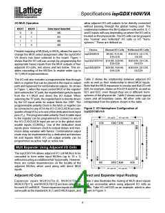
MUX Expander Using Adjacent I/O Cells
The ispGDXV/VA allows adjacent I/O cell MUXes to be
cascaded to form wider input MUXes (up to 16 x 1)
without incurring an additional full Tpd penalty. However,
there are certain dependencies on the locality of the
adjacent MUXes when used along with direct MUX
inputs.
B0
B19 B20
B39
I/O cell 79 I/O cell 80
Direct and Expander Input Routing
Adjacent I/O Cells
Table 2 also illustrates the routing of MUX direct inputs
that are accessible when using adjacent I/O cells as
inputs. Take I/O cell D23 as an example, which is also
shown in Figure 3.
Expansion inputs MUXOUT[n-2], MUXOUT[n-1],
MUXOUT[n+1], and MUXOUT[n+2] are fuse-selectable
for each I/O cell MUX. These expansion inputs share the
samepathasthestandardA, B, CandDMUXinputs, and
4

 LATTICE [ LATTICE SEMICONDUCTOR ]