Specifications ispGDX160V/VA
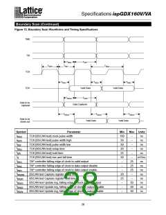
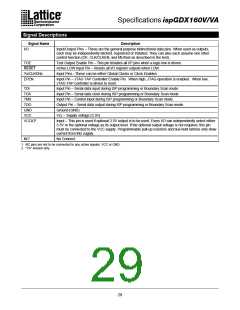
Boundary Scan
The ispGDXV/VA devices provide IEEE1149.1a test allows customers using boundary scan test to have full
capability and ISP programming through a standard test capability with only a single BSDL file.
Boundary Scan Test Access Port (TAP) interface.
The ispGDXV/VA devices are identified by the 32-bit
The boundary scan circuitry on the ispGDXV/VA Family JTAG IDCODE register. The device ID assignments are
operates independently of the programmed pattern. This listed in Table 4.
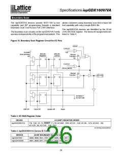
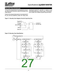
Figure 10. Boundary Scan Register Circuit for I/O Pins
HIGHZ
EXTEST
SCANIN
(from previous
cell
TOE
BSCAN
Registers
BSCAN
Latches
Normal
Function
OE
0
1
D
D
D
Q
Q
Q
D
Q
EXTEST
PROG_MODE
Normal
Function
0
1
I/O Pin
D
Q
SCANOUT
(to next cell)
Shift DR
Clock DR
Update DR
Reset
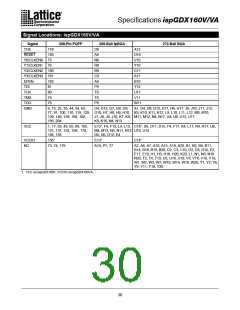
Table 3. I/O Shift Register Order
DEVICE
I/O SHIFT REGISTER ORDER
ispGDX160V/VA
TDI, TOE, Y2, Y3, RESET, Y1, Y0, I/O B20 .. B39, I/O C0 .. C39, I/O D0 .. D19, I/O B19 .. B0,
I/O A39.. A0, I/O D39 .. D20, TDO
I/O Shift Reg Order/ispGDXVA
Table 4. ispGDX160V/VA Device ID Codes
DEVICE
ispGDX160V
ispGDX160VA
32-BIT BOUNDARY SCAN ID CODE
0000, 0000, 0011, 0101, 0011, 0000, 0100, 0011
0001, 0000, 0011, 0101, 0011, 0000, 0100, 0011
ID Code/GDX160V/VA
26

 LATTICE [ LATTICE SEMICONDUCTOR ]