28
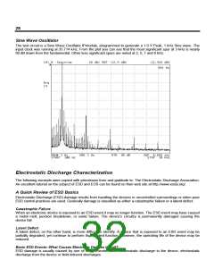
Sine Wave Oscillator
The test circuit is a Sine Wave Oscillator IPmodule, programmed to generate a 1.0 V Peak, 1 kHz Sine wave. The
input clock was running at 35.714 kHz. From the plot you can see that the most significant spur at 3 kHz is nearly
60 dB down from the fundamental. Other less significant spurs are noted at 2, 5, 7 and 9 kHz.
Electrostatic Discharge Characterization
The following excerpts were copied with permission from and gratitude to: The Electrostatic Discharge Association.
An excellent tutorial on the subject of ESD and EOS can be found on their web site at http://www.esda.org/.
A Quick Review of ESD Basics
Electrostatic Discharge (ESD) damage results from handling the devices in uncontrolled surroundings or when poor
ESD control practices are used. Generally damage is classified as either a catastrophic failure or a latent defect.
Catastrophic Failure
When an electronic device is exposed to an ESD event it may no longer function. The ESD event may have caused
a metal melt, junction breakdown, or oxide failure. The device's circuitry is permanently damaged causing the
device fail.
Latent Defect
A latent defect, on the other hand, is more difficult to identify. A device that is exposed to an ESD event may be
partially degraded, yet continue to perform its intended function. However, the operating life of the device may be
reduced.
Basic ESD Events--What Causes Electronic Devices to Fail?
ESD damage is usually caused by one of three events: direct electrostatic discharge to the device; electrostatic
discharge from the device or field induced discharges.

 LATTICE [ LATTICE SEMICONDUCTOR ]