ML145156
LANSDALE Semiconductor, Inc.
ML145156
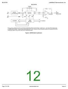
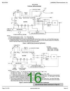
TYPICAL APPLICATIONS
+ 12 V
LOCK DETECT SIGNAL
3.2 MHz
NOTES 1
AND 2
FM B +
+ 12 V
AM B +
+ V
OSC
OSC
RA2 RA1 RA0 LD SW1 SW2
in
out
OPTIONAL
LOOP
ERROR SIGNAL
PD
out
V
V
DD
–
+
φ
ML145156
R
SS
VCO
REF
φ
V
out
1/2 MC1458
NOTE 3
f
CLK
DATA
ENB
in
MC
KEY–
BOARD
CMOS MPU/MCU
ML12019
20/21 DUAL MODULUS PRESCALER
÷
TO DISPLAY DRIVER (e.g., MC14489)
NOTES:
1. For AM: channel spacing = 5 kHz,
2. For FM: channel spacing = 25 kHz,
÷
R =
÷
640 (code 100).
÷ 128 (code 010).
÷
R =
3. Theφ andφ outputsarefedtoanexternalcombiner/loopfilter.SeethePhase–LockedLoop–Low–PassFilterDesignpage
R
V
for additional information. The φ and φ outputs swing rail–to–rail. Therefore, the user should be careful not to exceed the
R
V
common mode input range of the op amp used in the combiner/loop filter.
Figure 1. AM/FM Radio Broadcast Synthesizer
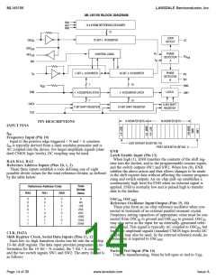
3.2 MHz (NOTE 3)
VCO RANGE
NAV = 01
COM = 10
NAV: 97.300 – 107.250 MHz
COM–T: 118.000 – 135.975 MHz
COM–R: 139.400 – 157.375 MHz
LOCK DETECT SIGNAL
+ V
OSC
OSC
out
RA2 RA1 RA0 LD SW1 SW2
in
PD
out
V
V
DD
–
+
ML145156
φ
R
SS
VCO
REF
φ
V
out
MC33171
NOTE 5
f
CLK
DATA
ENB
in
MC
CMOS MPU/MCU
R/T
ML12016 (NOTES 2 AND 4)
40/41 DUAL MODULUS PRESCALER
÷
CHANNEL
TO DISPLAY DRIVER
SELECTION
(e.g., MC14489)
NOTES:
1. For NAV: f = 50 kHz,
÷
R = 64 using 10.7 MHz lowside injection, N
= 1946 – 2145.
total
R
For COM–T: f = 25 kHz,
÷
÷
R = 128, N
= 4720 – 5439.
R
total
R = 128, using 21.4 MHz highside injection, N
For COM–R: f = 25 kHz,
= 5576 – 6295.
R
total
32/33 dual modulus approach is provided by substituting an ML12015 for the ML12016.The devices are pin equivalent.
3. A 6.4 MHz oscillator crystal can be used by selecting R = 128 (code 010) for NAV and R = 256 (code 011) for COM.
4. ML12013 + MC10131 combination may also be used to form the 40/41 prescale.r
5. The φ and φ outputs are fed to an external combiner/loop filter. See the Phase–Locked Loop – Low–Pass Filter Design
2. A
÷
÷
÷
÷
R
V
page for additional information.The φ and φ outputs swing rail–to–rail.Therefore, the user should be careful not to exceed
R
V
the common mode input range of the op amp used in the combiner/loop filter.
Figure 2. Avionics Navigation or Communication Synthesizer
ML145156 Data Sheet Continued on Page 23
Page 16 of 35
www.lansdale.com
Issue A

 LANSDALE [ LANSDALE SEMICONDUCTOR INC. ]