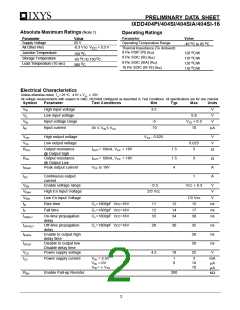
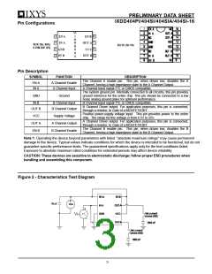
PRELIMINARY DATA SHEET
IXDD404PI/404SI/404SIA/404SI-16
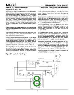
TTL to High Voltage CMOS Level Translation
The enable (EN) input to the IXDD404 is a high voltage
CMOS logic level input where the EN input threshold is ½
V , and may not be compatible with 5V CMOS or TTL input
leCvCels. The IXDD404 EN input was intentionally designed
for enhanced noise immunity with the high voltage CMOS
logic levels. In a typical gate driver application, VCC =15V
and the EN input threshold at 7.5V, a 5V CMOS logical high
input applied to this typical IXDD404 application’s EN input
will be misinterpreted as a logical low, and may cause
undesirable or unexpected results. The note below is for
optional adaptation of TTL or 5V CMOS levels.
Supply Bypassing and Grounding Practices,
Output Lead inductance
When designing a circuit to drive a high speed MOSFET
utilizing the IXDD404, it is very important to keep certain design
criteria in mind, in order to optimize performance of the driver.
Particular attention needs to be paid to Supply Bypassing,
Grounding, and minimizing the Output Lead Inductance.
Say,forexample,weareusingtheIXDD404tochargea2500pF
capacitive load from 0 to 25 volts in 25ns.
Using the formula: I= ∆V C / ∆t, where ∆V=25V C=2500pF &
∆t=25ns we can determine that to charge 2500pF to 25 volts in
25nswilltakeaconstantcurrentof2.5A. (Inreality, thecharging
current won’t be constant, and will peak somewhere around
4A).
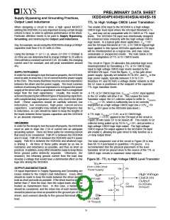
The circuit in Figure 28 alleviates this potential logic level
misinterpretation by translating a TTL or 5V CMOS logic
input to high voltage CMOS logic levels needed by the
IXDD404 EN input. From the figure, VCC is the gate driver
power supply, typically set between 8V to 20V, and VDD is the
logic power supply, typically between 3.3V to 5.5V.
Resistors R1 and R2 form a voltage divider network so that
the Q1 base is positioned at the midpoint of the expected
TTL logic transition levels.
SUPPLYBYPASSING
In order for our design to turn the load on properly, the IXDD404
must be able to draw this 2.5A of current from the power supply
in the 25ns. This means that there must be very low impedance
between the driver and the power supply. The most common
method of achieving this low impedance is to bypass the power
supply at the driver with a capacitance value that is a magnitude
larger than the load capacitance. Usually, this would be
achievedbyplacingtwodifferenttypesofbypassingcapacitors,
with complementary impedance curves, very close to the driver
itself. (These capacitors should be carefully selected, low
inductance, low resistance, high-pulse current-service
capacitors). Lead lengths may radiate at high frequency due
to inductance, so care should be taken to keep the lengths of
the leads between these bypass capacitors and the IXDD404
to an absolute minimum.
A TTL or 5V CMOS logic low, V
=~<0.8V, input applied
to the Q1 emitter will drive it on.TTTLLhOiWs causes the level
translator output, the Q1 collector output to settle to
V
+ V
=<~2V, which is sufficiently low to be correctlyCESATQ1
inteTrTpLrLeOWted as a high voltage CMOS logic low (<1/3VCC=5V
for VCC =15V given in the IXDD404 data sheet.)
A TTL high, VTTLHIGH=>~2.4V, or a 5V CMOS high,
V5VCMOSHIGH=~>3.5V, applied to the EN input of the circuit in
Figure 28 will cause Q1 to be biased off. This results in Q1
collector being pulled up by R3 to V =15V, and provides a
high voltage CMOS logic high outpuCt.C The high voltage
CMOS logical EN output applied to the IXDD404 EN input
will enable it, allowing the gate driver to fully function as a
±4 Amp output driver.
GROUNDING
In order for the design to turn the load off properly, the IXDD404
must be able to drain this 2.5A of current into an adequate
grounding system. There are three paths for returning current
that need to be considered: Path #1 is between the IXDD404
and it’s load. Path #2 is between the IXDD404 and it’s power
supply. Path #3 is between the IXDD404 and whatever logic
is driving it. All three of these paths should be as low in
resistance and inductance as possible, and thus as short as
practical. In addition, every effort should be made to keep these
three ground paths distinctly separate. Otherwise, (for
instance), the returning ground current from the load may
develop a voltage that would have a detrimental effect on the
logic line driving the IXDD404.
The total component cost of the circuit in Figure 28 is less
than $0.10 if purchased in quantities >1K pieces. It is
recommended that the physical placement of the level
translator circuit be placed close to the source of the TTL or
CMOS logic circuits to maximize noise rejection.
Figure 28 - TTL to High Voltage CMOS Level Translator
CC
(FromGate Driver
Power Supply)
OUTPUTLEADINDUCTANCE
R3
10K
Of equal importance to Supply Bypassing and Grounding are
issues related to the Output Lead Inductance. Every effort
should be made to keep the leads between the driver and it’s
load as short and wide as possible. If the driver must be placed
farther than 2” from the load, then the output leads should be
treated as transmission lines. In this case, a twisted-pair
should be considered, and the return line of each twisted pair
should be placed as close as possible tothe ground pin of the
driver, and connect directly to the ground terminal of the
load.
High Voltage
V
DD
EN
CMOS
3.3K
(FromLogic
R1
Output
Power Supply)
Q1
(To IXDD404
EN Input)
2N3904
3.3K R2
or TTL
Input)
9

 IXYS [ IXYS CORPORATION ]