PRELIMINARY DATA SHEET
IXDD404PI/404SI/404SIA/404SI-16
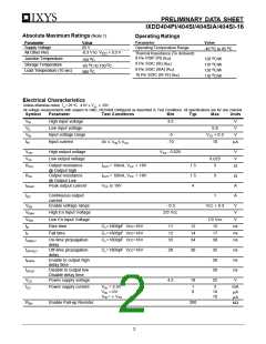
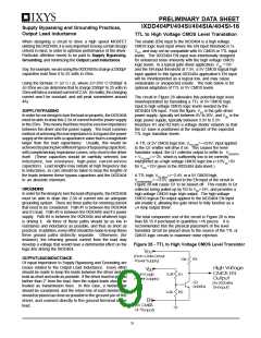
Pin Configurations
1
2
8
7
6
5
I
EN A
IN A
EN B
X
D
D
4
0
4
OUT A
SO8 (SI, SIA)
8 PIN DIP (PI)
SO16 (SI-16)
3
GND
IN B
VCC
4
OUT B
Pin Description
SYMBOL
FUNCTION
DESCRIPTION
The Channel A enable pin. This pin, when driven low, disables the A
Channel, forcing a high impedance state to the A Channel Output.
A Channel Input signal-TTL or CMOS compatible.
EN A
IN A
A Channel Enable
A Channel Input
The system ground pin. Internally connected to all circuitry, this pin provides
ground reference for the entire chip. This pin should be connected to a low
noise analog ground plane for optimum performance.
GND
Ground
IN B
B Channel Input
B Channel Input signal-TTL or CMOS compatible.
B Channel Driver output. For application purposes, this pin is connected,
through a resistor, to Gate of a MOSFET/IGBT.
OUT B
B Channel Output
Positive power-supply voltage input. This pin provides power to the entire
chip. The range for this voltage is from 4.5V to 25V.
VCC
OUT A
EN B
Supply Voltage
A Channel Output
B Channel Enable
A Channel Driver output. For application purposes, this pin is connected,
through a resistor, to Gate of a MOSFET/IGBT.
The Channel B enable pin. This pin, when driven low, disables the B
Channel, forcing a high impedance state to the B Channel Output.
Note 1: Operating the device beyond parameters with listed “absolute maximum ratings” may cause permanent
damage to the device. Typical values indicate conditions for which the device is intended to be functional, but do not
guarantee specific performance limits. The guaranteed specifications apply only for the test conditions listed.
Exposure to absolute maximum rated conditions for extended periods may affect device reliability.
CAUTION: These devices are sensitive to electrostatic discharge; follow proper ESD procedures when
handling and assembling this component.
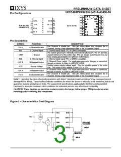
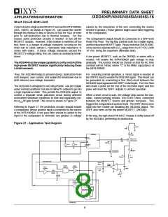
Figure 2 - Characteristics Test Diagram
IN
V
3

 IXYS [ IXYS CORPORATION ]