PRELIMINARY DATA SHEET
IXDD404PI/404SI/404SIA/404SI-16
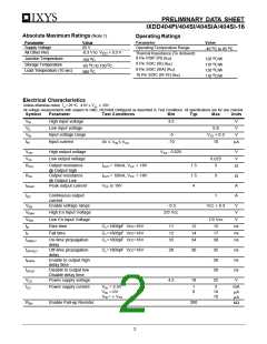
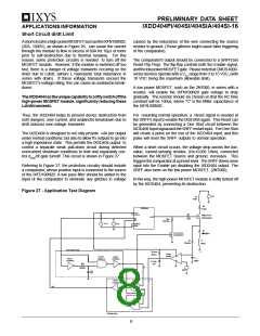
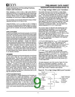
Absolute Maximum Ratings (Note 1)
Operating Ratings
Parameter
Value
-40 C to 85
Parameter
Value
Operating Temperature Range
o
o
Supply Voltage
All Other Pins
Junction Temperature
Storage Temperature
Lead Temperature (10 sec)
25 V
C
-0.3 V to V
+ 0.3 V
Thermal Impedance (To Ambient)
CC
o
θ
θ
8 Pin PDIP (PI) (
8 Pin SOIC (SI) (
)
JA
o
120 C/W
150 C
o
)
JA
o
o
110 C/W
-65 C to 150 C
o
θ
8 Pin SOIC (SIA) (
)
JA
120 C/W
o
300 C
o
θ
16 Pin SOIC (SI-16) (
)
JA
110 C/W
Electrical Characteristics
Unless otherwise noted, TA = 25 oC, 4.5V ≤ VCC ≤ 25V .
All voltage measurements with respect to GND. IXDD404 configured as described in Test Conditions. All specifications are for one channel.
Symbol
VIH
VIL
VIN
IIN
Parameter
Test Conditions
Min
3.5
Typ
Max
Units
High input voltage
Low input voltage
Input voltage range
Input current
V
V
V
0.8
VCC + 0.3
10
-5
-10
≤
≤
µ
A
0V VIN VCC
VOH
VOL
ROH
High output voltage
Low output voltage
VCC - 0.025
V
V
Ω
0.025
3
Output resistance
IOUT = 10mA, VCC = 18V
IOUT = 10mA, VCC = 18V
VCC is 18V
1.5
1.5
4
@ Output high
ROL
IPEAK
IDC
Output resistance
@ Output Low
3
Ω
A
A
Peak output current
Continuous output
current
Enable voltage range
High En Input Voltage
Low En Input Voltage
Rise time
1
VEN
VENH
VENL
tR
tF
tONDLY
- 0.3
2/3 Vcc
Vcc + 0.3
V
V
V
ns
ns
ns
1/3 Vcc
15
CL=1800pF Vcc=18V
CL=1800pF Vcc=18V
CL=1800pF Vcc=18V
11
12
33
12
14
34
Fall time
17
38
On-time propagation
delay
tOFFDLY
tENOH
tDOLD
Off-time propagation
delay
CL=1800pF Vcc=18V
28
30
35
30
30
25
ns
ns
ns
Enable to output high
delay time
Disable to output low
Disable delay time
Power supply voltage
VCC
ICC
4.5
18
1
0
V
Power supply current
VIN = 3.5V
VIN = 0V
3
mA
10
10
µ
µ
A
A
VIN = + VCC
REN
Enable Pull-up Resistor
200
Ω
k
2

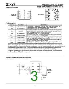
 IXYS [ IXYS CORPORATION ]