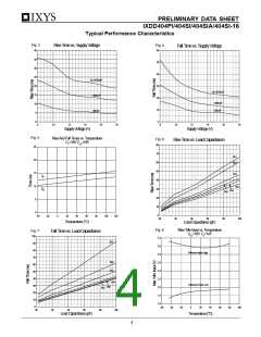
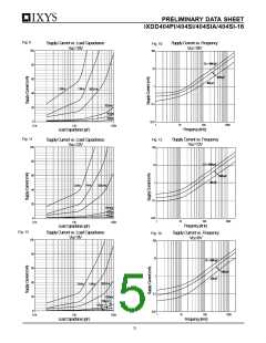
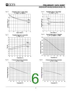
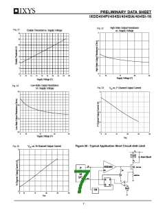
PRELIMINARY DATA SHEET
IXDD404PI/404SI/404SIA/404SI-16
APPLICATIONS INFORMATION
Short Circuit di/dt Limit
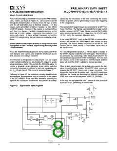
Ashortcircuitinahigh-powerMOSFETsuchastheIXFN100N20,
(20A, 1000V), as shown in Figure 26, can cause the current
through the module to flow in excess of 60A for 10µs or more
prior to self-destruction due to thermal runaway. For this
reason, some protection circuitry is needed to turn off the
MOSFET module. However, if the module is switched off too
fast, there is a danger of voltage transients occuring on the
drain due to Ldi/dt, (where L represents total inductance in
series with drain). If these voltage transients exceed the
MOSFET's voltage rating, this can cause an avalanche break-
down.
caused by the inductance of the wire connecting the source
resistor to ground. (Those glitches might cause false triggering
of the comparator).
The comparator's output should be connected to a SRFF(Set
Reset Flip Flop). The flip-flop controls both the Enable signal,
andthelowpowerMOSFETgate. PleasenotethatCMOS4000-
series devices operate with a VCC range from 3 to 15 VDC, (with
18 VDC being the maximum allowable limit).
A low power MOSFET, such as the 2N7000, in series with a
resistor, will enable the IXFN100N20 gate voltage to drop
gradually. The resistor should be chosen so that the RC time
constant will be 100us, where "C" is the Miller capacitance of
the IXFN100N20.
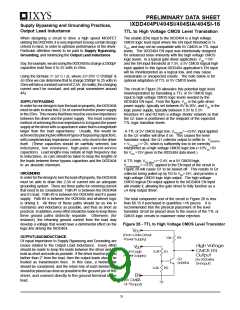
TheIXDD404hastheuniquecapabilitytosoftlyswitchoffthe
high-power MOSFET module, significantly reducing these
Ldi/dttransients.
Thus, the IXDD404 helps to prevent device destruction from
both dangers; over-current, and avalanche breakdown due to
di/dt induced over-voltage transients.
For resuming normal operation, a Reset signal is needed at
the SRFF's input to enable the IXDD404 again. This Reset can
be generated by connecting a One Shot circuit between the
IXDD408 Input signal and the SRFF restart input. The One Shot
will create a pulse on the rise of the IXDD404 input, and this
pulse will reset the SRFF outputs to normal operation.
The IXDD404 is designed to not only provide ±4A per output
under normal conditions, but also to allow it's outputs to go into
a high impedance state. This permits the IXDD404 output to
control a separate weak pull-down circuit during detected
overcurrent shutdown conditions to limit and separately con-
trol dVGS/dt gate turnoff. This circuit is shown in Figure 27.
When a short circuit occurs, the voltage drop across the low-
value, current-sensing resistor, (Rs=0.005 Ohm), connected
between the MOSFET Source and ground, increases. This
triggers the comparator at a preset level. The SRFF drives a low
input into the Enable pin disabling the IXDD404 output. The
SRFF also turns on the low power MOSFET, (2N7000).
Referring to Figure 27, the protection circuitry should include
a comparator, whose positive input is connected to the source
of the IXFD100N20. A low pass filter should be added to the
input of the comparator to eliminate any glitches in voltage
In this way, the high-power MOSFET module is softly turned off
by the IXDD404, preventing its destruction.
Figure 27 - Application Test Diagram
+
VB
Ld
10uH
-
Rd
0.1ohm
IXDD404
VCC
Rg
VCCA
High_Power
OUT
IXFN100N20
Rs
IN
1ohm
Rsh
EN
1600ohm
+
-
+
-
VCC
VIN
DGND
SUB
Low_Power
2N7002/PLP
Ls
20nH
R+
10kohm
One ShotCircuit
0
Rcomp
5kohm
Comp
LM339
+
V+
NAND
NOT2
C+
100pF
NOT1
CD4011A
CD4049A
V-
-
CD4049A
Ccomp
1pF
Ros
+
R
1Mohm
REF -
Cos
1pF
Q
NOT3
NOR1
S
CD4049A
CD4001A
EN
NOR2
CD4001A
SR Flip-Flop
8

 IXYS [ IXYS CORPORATION ]