®
IS42S32200
ISSI
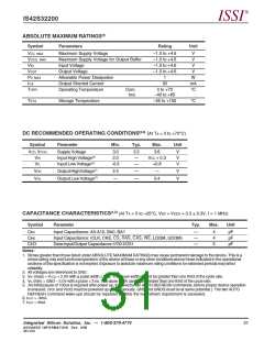
ABSOLUTE MAXIMUM RATINGS(1)
Symbol
Parameters
Rating
Unit
VCC MAX
VCCQ MAX
VIN
Maximum Supply Voltage
Maximum Supply Voltage for Output Buffer
Input Voltage
Output Voltage
Allowable Power Dissipation
Output Shorted Current
–1.0 to +4.6
–1.0 to +4.6
–1.0 to +4.6
–1.0 to +4.6
1
50
0 to +70
–40 to +85
V
V
V
VOUT
V
PD MAX
ICS
W
mA
°C
TOPR
Operating Temperature
Com.
Ind.
TSTG
Storage Temperature
–55 to +150
°C
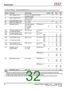
DC RECOMMENDED OPERATING CONDITIONS(2,5) (At TA = 0 to +70°C)
Symbol
Parameter
Min.
Typ.
Max.
Unit
VCC,VCCQ
VIH
SupplyVoltage
3.0
2.0
-0.3
3.3
—
—
3.6
VCC + 0.3
+0.8
V
V
V
Input High Voltage(3)
Input Low Voltage(4)
VIL
VOH
VOL
OutputHighVoltage(7)
Output Low Voltage(7)
2.4
—
—
—
—
V
V
0.4
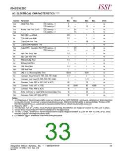
CAPACITANCE CHARACTERISTICS(1,2) (At TA = 0 to +25°C, Vcc = VccQ = 3.3 0.3V, f = 1 MHz)
Symbol
Parameter
Typ.
Max.
Unit
CIN1
CIN2
CI/O
Input Capacitance: A0-A10, BA0, BA1
Input Capacitance: (CLK, CKE, CS, RAS, CAS, WE, LDQM, UDQM)
DataInput/OutputCapacitance:I/O0-I/O31
—
—
—
4
4
5
pF
pF
pF
Notes:
1. Stress greater than those listed under ABSOLUTE MAXIMUM RATINGS may cause permanent damage to the device. This is a
stress rating only and functional operation of the device at these or any other conditions above those indicated in the operational
sections of this specification is not implied. Exposure to absolute maximum rating conditions for extended periods may affect
reliability.
2. All voltages are referenced to GND.
3. VIH (max) = VCCQ + 2.0V with a pulse width ≤ 3 ns. The pluse width cannot be greater than one third of the cycle rate.
4. VIL (min) = GND – 2.0V with a pulse < 3 ns. The pluse width cannot be greater than one third of the cycle rate.
5. An initial pause of 100us is required after power up, followed by two AUTO REFRESH commands, before proper device operation
is ensured. (Vcc and VccQ must be powered up simultaneously. GND and GNDQ must be at same potential.) The two AUTO
REFRESH command wake-ups should be repeated anytime the tREF refresh requirement is exceeded.
6. IOUT = -4mA
7. IOUT = 4mA
Integrated Silicon Solution, Inc. — 1-800-379-4774
31
ADVANCE INFORMATION Rev. 00B
08/14/03

 ISSI [ INTEGRATED SILICON SOLUTION, INC ]