IRS20124S(PbF)
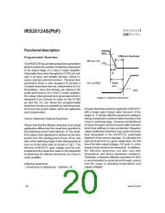
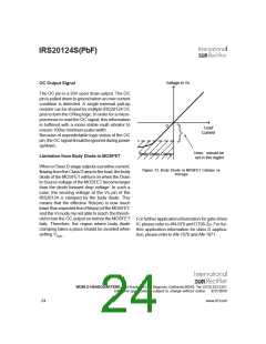
Voltage in Vs
OC Output Signal
The OC pin is a 20V open drain output. The OC
pin is pulled down to ground when an over current
condition is detected. A single external pull-up
resistor can be shared by multiple IRS20124 OC
pins to form the ORing logic. In order for a micro-
processor to read the OC signal, this information
is buffered with a mono stable multi vibrator to
ensure 100ns minimum pulse width.
0
Load
Current
Because of unpredictable logic status of the OC
pin, the OC signal should be ignored during power
up/down.
}
Vsoc- should be
set in this region
Body Diode Clamp
Limitation from Body Diode in MOSFET
When a Class D stage outputs a positive current,
flowing from the Class D amp to the load, the body
diode of the MOSFET will turn on when the Drain
to Source voltage of the MOSFET become larger
than the diode forward drop voltage. In such a
case, the sensing voltage at the Vs pin of the
IRS20124 is clamped by the body diode. This
means that the effective Rds(on) is now much
lower than expected from Rds(on) of the MOSFET,
and the Vs node my not able to reach the thresh-
old to turn the OC output on before the MOSFET
fails. Therefore, the region where body diode
clamping takes a place should be avoided when
Figure 13. Body Diode in MOSFET Clamps vs
Voltage
For further application information for gate driver
IC please refer to AN-978 and DT98-2a. For fur-
ther application information for class D applica-
tion, please refer to AN-1070 and AN-1071.
setting VSOC-
.
WORLD HEADQUARTERS: 233 Kansas St., El Segundo, California 90245 Tel: (310) 322 3331
Data and specifications subject to change without notice.
9/21/2005
24
www.irf.com

 INFINEON [ Infineon ]