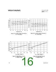
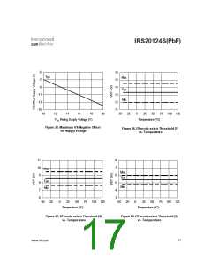
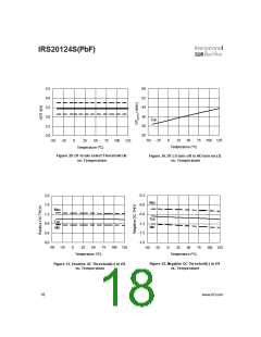
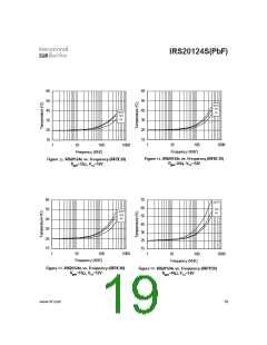
IRS20124S(PbF)
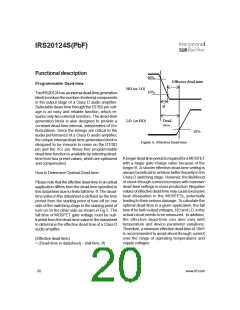
DT/SD pin
Dead-
time
R1
R2
DT/SD
voltage
DT/SD pin provides two functions: 1) setting dead-
time and 2) shutdown. The IRS20124 determines
its operation mode based on the voltage applied
to the DT/SD pin. An internal comparator
translates which mode is being used by comparing
internal reference voltages. Threshold voltages for
each mode are set internally by a resistive voltage
divider off Vcc, negating the need of using a precise
absolute voltage to set the mode.
mode
DT1
<10k
3.3k
5.6k
8.2k
Open
8.2k
4.7k
3.3k
1.0 x Vcc
0.71 x Vcc
0.46 x Vcc
0.29 x Vcc
DT2
DT3
DT4
Table 1. Suggested resistor values for dead-time
settings
Shutdown
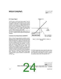
The relationship between the operation mode and
the voltage at DT/SD pin is illustrated in the Fig.7.
Since IRS20124 has internal dead-time genera-
tion, independent inputs for HO and LO are no
longer provided. Shutdown mode is the only way
to turn off both MOSFETs simultaneously to pro-
tect them from over current conditions. If the DT/
SD pin detects an input voltage below the thresh-
old, VDT4, the IRS20124 will output 0V at both HO
and LO outputs, forcing the switching output node
to go into a high impedance state.
Operational Mode
15nS
25nS
Dead-time
35nS
45nS
Over Current Sensing
Shutdown
VDT
0.23xVcc 0.36xVcc 0.57xVcc 0.89xVcc Vcc
In order to protect the power MOSFET, IRS20124
has a feature to detect over current conditions,
which can occur when speaker wires are shorted
together. The over current shutdown feature can
be configured by combining the current sensing
function with the shutdown mode via the DT/SD pin.
Figure 7. Dead-time Settings vs V
Voltage
DT
Design Example
Table 1 shows suggested values of resistance for
setting the dead-
IRS20124
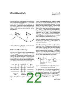
Load Current Direction in Class D Audio
Application
time. Resistors with
>0.5mA
Vcc
up to 5% tolerance
can be used if these
listed values are fol-
lowed.
R1
R2
In a Class D audio amplifier, the direction of the
load current alternates according to the audio in-
put signal. An over current condition can therefore
happen during either a positive current cycle or a
negative current cycle. Fig.9 shows the rela-
DT/SD
COM
Figure 8. External Resistor
www.irf.com
21

 INFINEON [ Infineon ]