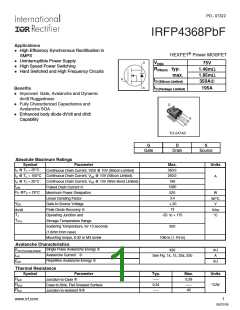
IRFP4368PbF
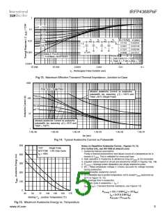
Driver Gate Drive
P.W.
P.W.
Period
Period
D =
D.U.T
+
*
=10V
V
GS
Circuit Layout Considerations
• Low Stray Inductance
• Ground Plane
• Low Leakage Inductance
Current Transformer
-
D.U.T. I Waveform
SD
+
-
Reverse
Recovery
Current
Body Diode Forward
Current
di/dt
-
+
D.U.T. V Waveform
DS
Diode Recovery
dv/dt
V
DD
VDD
Re-Applied
Voltage
• dv/dt controlled by RG
RG
+
-
Body Diode
Forward Drop
• Driver same type as D.U.T.
• ISD controlled by Duty Factor "D"
• D.U.T. - Device Under Test
Inductor Current
Inductor Curent
I
SD
Ripple
≤ 5%
* VGS = 5V for Logic Level Devices
Fig 20. Peak Diode Recovery dv/dt Test Circuit for N-Channel
HEXFET® Power MOSFETs
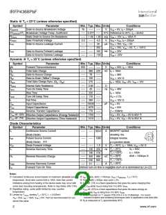
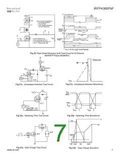
V
(BR)DSS
15V
t
p
DRIVER
+
L
V
DS
D.U.T
R
G
V
DD
-
I
A
AS
V
20V
GS
0.01Ω
t
p
I
AS
Fig 21b. Unclamped Inductive Waveforms
Fig 21a. Unclamped Inductive Test Circuit
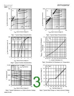
LD
VDS
VDS
90%
+
-
VDD
10%
VGS
D.U.T
VGS
Pulse Width < 1µs
Duty Factor < 0.1%
td(on)
td(off)
tr
tf
Fig 22a. Switching Time Test Circuit
Fig 22b. Switching Time Waveforms
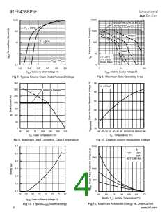
Id
Vds
Vgs
L
VCC
DUT
Vgs(th)
0
1K
Qgs1
Qgs2
Qgd
Qgodr
Fig 23a. Gate Charge Test Circuit
Fig 23b. Gate Charge Waveform
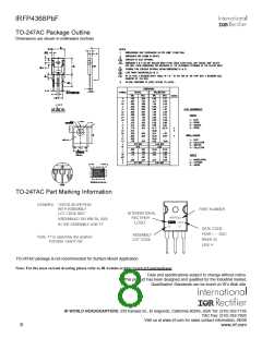
www.irf.com
7

 INFINEON [ Infineon ]