IRFP4368PbF
Static @ TJ = 25°C (unless otherwise specified)
Symbol
V(BR)DSS
Parameter
Drain-to-Source Breakdown Voltage
Breakdown Voltage Temp. Coefficient
Static Drain-to-Source On-Resistance
Gate Threshold Voltage
Min. Typ. Max. Units
75 ––– –––
––– 0.077 ––– V/°C Reference to 25°C, ID = 5mAd
Conditions
VGS = 0V, ID = 250µA
V
∆V(BR)DSS/∆TJ
RDS(on)
––– 1.46 1.85
VGS = 10V, ID = 195A g
mΩ
V
VGS(th)
2.0
–––
4.0
20
VDS = VGS, ID = 250µA
VDS = 75V, VGS = 0V
VDS = 75V, VGS = 0V, TJ = 125°C
VGS = 20V
V
IDSS
Drain-to-Source Leakage Current
––– –––
µA
––– ––– 250
––– ––– 100
––– ––– -100
IGSS
Gate-to-Source Forward Leakage
Gate-to-Source Reverse Leakage
nA
GS = -20V
Dynamic @ TJ = 25°C (unless otherwise specified)
Symbol
gfs
Parameter
Forward Transconductance
Total Gate Charge
Min. Typ. Max. Units
Conditions
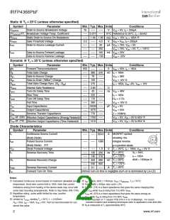
VDS = 50V, ID = 195A
650 ––– –––
S
Qg
––– 380 570
nC ID = 195A
VDS = 38V
Qgs
Qgd
Qsync
Gate-to-Source Charge
–––
79
–––
Gate-to-Drain ("Miller") Charge
Total Gate Charge Sync. (Qg - Qgd)
––– 105 –––
––– 275 –––
VGS = 10V g
ID = 195A, VDS =0V, VGS = 10V
RG(int)
td(on)
–––
Ω
Internal Gate Resistance
Turn-On Delay Time
Rise Time
0.80 –––
43 –––
–––
ns VDD = 49V
ID = 195A
RG = 2.7Ω
VGS = 10V g
tr
––– 220 –––
––– 170 –––
––– 260 –––
––– 19230 –––
––– 1670 –––
––– 770 –––
––– 1700 –––
––– 1410 –––
td(off)
Turn-Off Delay Time
Fall Time
tf
Ciss
Input Capacitance
Output Capacitance
Reverse Transfer Capacitance
pF
V
GS = 0V
Coss
VDS = 50V
Crss
ƒ = 100kHz
Coss eff. (ER)
Coss eff. (TR)
V
GS = 0V, VDS = 0V to 60V i
GS = 0V, VDS = 0V to 60V h
Effective Output Capacitance (Energy Related)
i
V
Effective Output Capacitance (Time Related)
h
Diode Characteristics
Symbol
Parameter
Min. Typ. Max. Units
Conditions
IS
Continuous Source Current
––– –––
A
MOSFET symbol
D
S
350
c
(Body Diode)
showing the
integral reverse
G
ISM
Pulsed Source Current
(Body Diode)ꢁdi
Diode Forward Voltage
Reverse Recovery Time
––– ––– 1280
p-n junction diode.
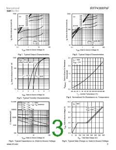
TJ = 25°C, IS = 195A, VGS = 0V g
VSD
trr
––– ––– 1.3
V
TJ = 25°C
TJ = 125°C
TJ = 25°C
TJ = 125°C
TJ = 25°C
VR = 64V,
––– 130 200
––– 140 210
––– 450 680
––– 530 800
ns
IF = 195A
di/dt = 100A/µs g
Qrr
Reverse Recovery Charge
nC
IRRM
ton
Reverse Recovery Current
Forward Turn-On Time
–––
9.1
–––
A
Intrinsic turn-on time is negligible (turn-on is dominated by LS+LD)
Notes:
Calculated continuous current based on maximum allowable junction
temperature. Bond wire current limit is 195A. Note that current
limitations arising from heating of the device leads may occur with
ISD ≤ 195A, di/dt ≤ 1740A/µs, VDD ≤ V(BR)DSS, TJ ≤ 175°C.
ꢀ Pulse width ≤ 400µs; duty cycle ≤ 2%.
Coss eff. (TR) is a fixed capacitance that gives the same charging time
some lead mounting arrangements. Refer to App Notes (AN-1140).
Repetitive rating; pulse width limited by max. junction
temperature.
as Coss while VDS is rising from 0 to 80% VDSS
Coss eff. (ER) is a fixed capacitance that gives the same energy as
Coss while VDS is rising from 0 to 80% VDSS
When mounted on 1" square PCB (FR-4 or G-10 Material). For recom
.
.
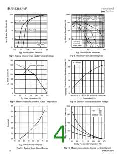
Limited by TJmax, starting TJ = 25°C, L = 0.022mH
mended footprint and soldering techniques refer to application note #AN-994.
Rθ is measured at TJ approximately 90°C.
RG = 25Ω, IAS = 195A, VGS =10V. Part not recommended for use
above this value.
2
www.irf.com

 INFINEON [ Infineon ]