IRF640N/S/L
RD
VDS
20
16
12
8
20
16
12
8
VGS
10V
D.U.T.
RG
+
-
VDD
Pulse Width ≤ 1 µs
Duty Factor ≤ 0.1 %
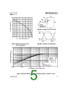
Fig 10a. Switching Time Test Circuit
V
DS
4
90%
4
0
25
50
50
75
75
100
100
125
125
150
150
175
175
0
25
°
, Case Temperature ( C)
10%
T
C
°
, Case Temperature ( C)
T
C
V
GS
t
t
r
t
t
f
d(on)
d(off)
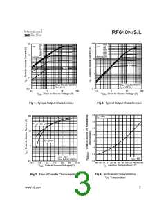
Fig 9. Maximum Drain Current Vs.
Fig 10b. Switching Time Waveforms
Case Temperature
10
1
D = 0.50
0.20
0.10
P
2
DM
0.1
t
0.05
1
t
0.02
0.01
2
SINGLE PULSE
(THERMAL RESPONSE)
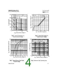
Notes:
1. Duty factor D = t / t
1
2. Peak T =P
x Z
+ T
C
J
DM
thJC
0.01
0.00001
0.0001
0.001
0.01
0.1
1
t , Rectangular Pulse Duration (sec)
1
Fig 11. Maximum Effective Transient Thermal Impedance, Junction-to-Case
www.irf.com
5

 INFINEON [ Infineon ]