IRF640N/S/L
Electrical Characteristics @ TJ = 25°C (unless otherwise specified)
Parameter
Min. Typ. Max. Units
200 ––– –––
Conditions
VGS = 0V, ID = 250µA
V(BR)DSS
Drain-to-Source Breakdown Voltage
V
∆V(BR)DSS/∆TJ Breakdown Voltage Temp. Coefficient ––– 0.25 ––– V/°C Reference to 25°C, ID = 1mA
RDS(on)
VGS(th)
gfs
Static Drain-to-Source On-Resistance
Gate Threshold Voltage
––– ––– 0.15
Ω
V
S
VGS = 10V, ID = 11A
2.0
6.8
––– 4.0
––– –––
VDS = VGS, ID = 250µA
Forward Transconductance
VDS = 50V, ID = 11A
VDS = 200V, VGS = 0V
VDS = 160V, VGS = 0V, TJ = 150°C
VGS = 20V
––– ––– 25
––– ––– 250
––– ––– 100
––– ––– -100
––– ––– 67
––– ––– 11
––– ––– 33
IDSS
Drain-to-Source Leakage Current
µA
nA
Gate-to-Source Forward Leakage
Gate-to-Source Reverse Leakage
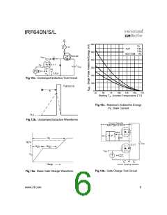
Total Gate Charge
IGSS
VGS = -20V
Qg
ID = 11A
Qgs
Qgd
td(on)
tr
Gate-to-Source Charge
Gate-to-Drain ("Miller") Charge
Turn-On Delay Time
Rise Time
nC VDS = 160V
VGS = 10V, See Fig. 6 and 13
–––
–––
–––
–––
10 –––
19 –––
23 –––
5.5 –––
VDD = 100V
ID = 11A
ns
td(off)
tf
Turn-Off Delay Time
Fall Time
RG = 2.5Ω
RD = 9.0Ω, See Fig. 10
Between lead,
6mm (0.25in.)
from package
D
LD
LS
Internal Drain Inductance
Internal Source Inductance
–––
–––
4.5 –––
nH
G
–––
7.5
and center of die contact
VGS = 0V
S
Ciss
Coss
Crss
Input Capacitance
––– 1160 –––
––– 185 –––
Output Capacitance
VDS = 25V
Reverse Transfer Capacitance
–––
53 –––
pF
ƒ = 1.0MHz, See Fig. 5
Source-Drain Ratings and Characteristics
Parameter
Continuous Source Current
(Body Diode)
Min. Typ. Max. Units
Conditions
MOSFET symbol
showing the
D
IS
18
72
––– –––
––– –––
A
G
ISM
Pulsed Source Current
(Body Diode)
integral reverse
S
p-n junction diode.
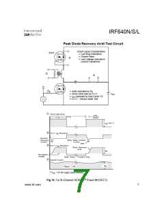
VSD
trr
Diode Forward Voltage
Reverse Recovery Time
Reverse Recovery Charge
Forward Turn-On Time
––– ––– 1.3
––– 167 251
V
TJ = 25°C, IS = 11A, VGS = 0V
TJ = 25°C, IF = 11A
ns
Qrr
ton
––– 929 1394 nC di/dt = 100A/µs
Intrinsic turn-on time is negligible (turn-on is dominated by LS+LD)
Thermal Resistance
Parameter
Junction-to-Case
Typ.
–––
Max.
1.0
Units
RθJC
RθCS
RθJA
RθJA
Case-to-Sink, Flat, Greased Surface
Junction-to-Ambient
Junction-to-Ambient (PCB mount)ꢀ
0.50
–––
–––
62
°C/W
–––
40
www.irf.com
2

 INFINEON [ Infineon ]