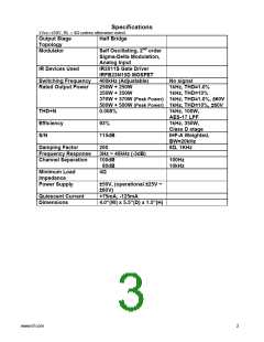
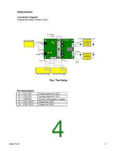
Functional Description
Feed back
+
V
C
C
Integrator
LT1220
Level Shifter
2N5401
IR2011S
Gate
LPF
Driver
GND
Comparator
74HC04
IRFB23N15
D
-V
C
C
-VCC
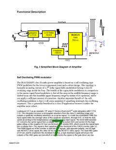
Fig. 3 Simplified Block Diagram of Amplifier
Self Oscillating PWM modulator
The IRAUDAMP1 class D audio power amplifier is based on a self oscillating type
PWM modulator for the lowest component count and a robust design. This topology is
basically an analog version of a 2nd order sigma delta modulation having a class D
switching stage inside the loop. The benefit of the sigma delta modulation in comparison
to the carrier signal based modulator is that all the error in the audible frequency range is
shifted away into the inaudible upper frequency range by nature of its operation, and it
can apply a sufficient amount of correction. Another important benefit of the self-
oscillating modulator is that it will cease operation if something interrupts the oscillating
sequences. This is generally beneficial in a class D application because it makes the
amplifier more robust.
Looking at CH-1 as an example, OP amp U1 forms a front end 2nd order integrator with C17 &
C18. This integrator receives a rectangular waveform from the class D switching stage and
outputs a quadratic oscillatory waveform as a carrier signal. To create the modulated PWM, the
input signal shifts the average value of this quadratic waveform, through R10, so that the duty
varies according to the instantaneous value of the analog input signal. The level shift transistor
Q1 converts the carrier signal from a voltage form into a current form and sends it to the logic
gates sitting on the negative DC bus via the level shift resistor R44, which conerts the signal back
into a voltage form. The signal is then quantized by the threshold of the CMOS inverter gate U2.
The PWM signal out of the inverter is split into two signals, with opposite polarity, one for high
side MOSFET drive signal, the other for the low side MOSFET drive signal. The dual AND gates
of U4 are used to implement the shutdown function, a high shutdown signal will ensure the
outputs of the AND gates are low which in turn ensures the inputs to the gate driver are low.
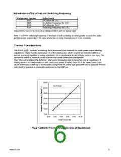
www.irf.com
6

 INFINEON [ Infineon ]