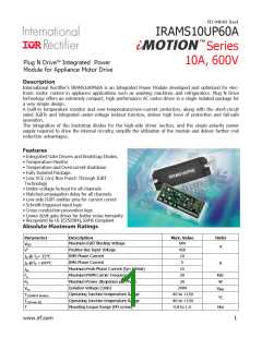
IRAMS10UP60A
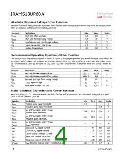
Absolute Maximum Ratings Driver Function
Absolute Maximum Ratings indicate substaines limits beyond which damage to the device may occur. All voltage param-
eters are absolute voltages referenced toVSS (Note 1)
Symbol
VS1,2,3
VB1,2,3
VDD
Definition
Min
-0.3
-0.3
-0.3
-0.3
-40
Max
600
20
Units
V
V
High Side offset voltage
High Side floating supply voltage
Low Side and logic fixed supply voltage
Input voltage LIN, HIN, T/ITRIP
Juction Temperature
20
V
VIN
7
V
TJ
150
°C
Recommended Operating Conditions Driver Function
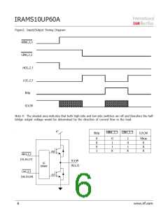
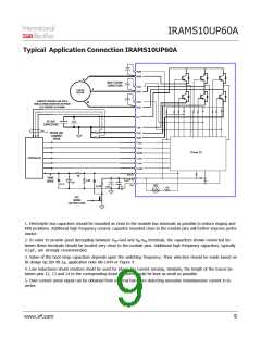
The Input/Output logic timing diagram is shown in Figure 1. For proper operation the device should be used within the
recommended conditions. All voltages are absolute referenced to VSS. The VS offset is tested with all supplies biased
at 15V differential (Note 1). All input pin (VIN ) and ITRIP are clamped with a 5.2V zener diode and pull-up resistor to
VDD
Symbol
VB1,2,3
VS1,2,3
VDD
Definition
Min
VS+12
Note 2
12
Max
VS+20
450
Units
High side floating supply voltage
High side floating supply offset voltage
Low side and logic fixed supply voltage
T/ITRIP input voltage
V
20
V
V
VITRIP
VIN
VSS
VSS+5
VSS+5
Logic input voltage LIN, HIN
VSS
Static Electrical Characteristics Driver Function
VBIAS (VCC, VBS1,2,3)=15V, unless otherwise specified. The VIN and IIN parameters are referenced to VSS and are appli-
cable to all six channels. (Note 1)
Symbol
VIN,th+
Definition
Positive going input threshold
Negative going input threshold
Min
3.0
---
Typ
---
Max
---
Units
V
V
VIN,th-
---
0.8
VCCUV+
VBSUV+
VCC and VBS supply undervoltage
Positive going threshold
10.6
10.4
---
11.1
10.9
0.2
11.6
11.4
---
V
V
V
VCCUV-
VBSUV-
VCC and VBS supply undervoltage
Negative going threshold
VCCUVH
VBSUVH
VCC and VBS supply undervoltage
Ilockout hysteresis
IQBS
IQCC
ILK
Quiescent VBS supply current
---
---
70
1.6
---
120
2.3
µA
mA
µA
µA
µA
V
Quiscent VCC supply current
Offset Supply Leakage Current
Input bias current (OUT=LO)
Input bias current (OUT=HI)
---
50
IIN+
IIN+
---
100
200
4.3
220
300
4.75
---
V(ITRIP
)
ITRIP threshold Voltage (OUT=HI or OUT=LO)
3.85
4
www.irf.com

 INFINEON [ Infineon ]