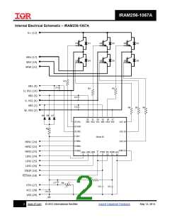
IRAM256-1067A
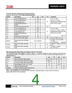
Static Electrical Characteristics Driver Function
VBIAS (VCC, VBS1,2,3)=15V, TJ=25ºC, unless otherwise specified. The VIN and IIN parameters are referenced to COM and are
applicable to all six channels. (Note 3)
Symbol
VIN,TH+
VIN,TH-
Description
Min
2.5
---
TYP
---
Max
---
Unit
V
Positive going input threshold for LIN, HIN, FLT/EN
Negative going input threshold for LIN, HIN, FLT/EN
VCC/VBS supply undervoltage, Positive going threshold
VCC/VBS supply undervoltage, Negative going threshold
VCC and VBS supply undervoltage lock-out hysteresis
Quiescent VBS supply current
---
0.8
11.6
11.4
---
V
VCCUV+, VBSUV+
VCCUV-, VBSUV-
VCCUVH, VBSUVH
IQBS
10.6
10.4
---
11.1
10.9
0.2
---
V
V
V
---
150
3.2
50
µA
mA
µA
µA
µA
µA
µA
V
IQCC
Quiescent VCC supply current
---
---
ILK
Offset Supply Leakage Current
---
---
IIN+
Input bias current VIN=3.3V for LIN, HIN, FLT/EN
Input bias current VIN=0V for LIN, HIN, FLT/EN
ITRIP bias current VITRIP=3.3V
---
100
---
195
---
IIN-
-1
ITRIP+
---
3.3
---
6
ITRIP-
ITRIP bias current VITRIP=0V
-1
---
VITRIP
ITRIP threshold Voltage
0.44
---
0.49
0.07
50
0.54
---
VITRIP_HYS
RFLT
ITRIP Input Hysteresis
V
Fault low on resistance
---
100
Ω
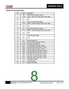
Dynamic Electrical Characteristics
VBIAS (VCC, VBS1,2,3)=15V, TJ=25ºC, unless otherwise specified. Dynamic parameters are guaranteed by design. (Note 3)
Symbol
Description
Min
Typ
Max
Unit
Conditions
Input to Output propagation
turn-on delay time (see Fig.12)
TON
---
---
1.15
µs
IC=4A, V+=300V
Input to Output propagation
turn-off delay time (see Fig.12)
TOFF
---
---
1.15
µs
TFILIN
Input filter time (HIN,LIN)
Input filter time (FLT/EN)
---
310
200
---
---
ns
ns
VIN=0 or VIN=5V
VEN=0 or VEN=5V
TFILEN
100
EN low to six switch turn-off
propagation delay (see fig. 3)
TEN
---
---
1.35
µs
VIN=0 or VIN=5V, VEN=0
VIN=0 or VIN=5V, VITRIP=5V
TFLT
ITRIP to Fault propagation delay
400
100
---
600
150
---
800
---
ns
ns
µs
TBLT-TRIP
TITRIP
ITRIP Blanking Time
VIN=0 or VIN=5V, VITRIP=5V
IC=4A, V+=300V
ITRIP to six switch turn-off
propagation delay (see fig. 2)
1.5
Internal Dead Time injected by
driver
Matching Propagation Delay
Time (On & Off) all channels
DT
220
---
290
40
360
75
ns
ns
VIN=0 or VIN=5V
MT
External dead time> 400ns
1.1
1
1.7
1.5
2.3
1.9
TC = 25°C
Post ITRIP to six switch turn-off
clear time (see fig. 2)
TFLT-CLR
ms
TC = 100°C
5
www.irf.com
© 2014 International Rectifier
Submit Datasheet Feedback
May 14, 2014

 INFINEON [ Infineon ]