IRAM256-1067A
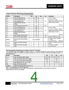
Inverter Section Switching Characteristics
VBIAS(VCC, VBS1,2,3)=15V, TJ=25°C unless otherwise specified.
Symbol
EON
Description
Min
---
Typ
170
60
Max
---
Unit
µJ
Conditions
IC=4A, V+=400V
VCC=15V, L=1.2mH
Energy losses include "tail" and
diode reverse recovery
Turn-On Switching Loss
Turn-Off Switching Loss
Total Switching Loss
EOFF
---
---
ETOT
---
230
---
Diode Reverse Recovery
energy
EREC
---
15
---
See CT1
TRR
Diode Reverse Recovery time
Turn-On Switching Loss
Turn-Off Switching Loss
Total Switching Loss
---
---
---
---
115
260
100
360
---
---
---
---
ns
IC=4A, V+=400V
VCC=15V, L=1.2mH, TJ=150°C
Energy losses include "tail" and
diode reverse recovery
EON
EOFF
ETOT
µJ
Diode Reverse Recovery
energy
EREC
---
40
---
See CT1
TRR
QG
Diode Reverse Recovery time
Turn-On IGBT Gate Charge
---
---
150
13
---
---
ns
nC
IC=6A, V+=400V, VGE=15V
TJ=150°C, IC=4A, VP=600V
V+= 450V,
Reverse Bias Safe Operating
Area
RBSOA
FULL SQUARE
VCC=+15V to 0V
See CT3
Short Circuit Safe Operating
Area
Short Circuit Safe Operating
Area
TJ=25°C, V+= 400V, VGE=+15V
to 0V
SCSOA
SCSOA
5
3
---
---
---
---
µs
µs
TJ=100°C, V+= 400V,
VGE=+15V to 0V
Recommended Operating Conditions Driver Function
The Input/Output logic timing diagram is shown in Figure 1. For proper operation the device should be used within the
recommended conditions. All voltages are absolute referenced to COM. The VS offset is tested with all supplies biased at 15V
differential (Note 3)
Symbol
VB1,2,3
VS1,2,3
VCC
Description
Min
TYP
Max
Unit
V
High side floating supply voltage
High side floating supply offset voltage
Low side and logic fixed supply voltage
Input voltage LIN, HIN, ITRIP, FLT/EN
High side PWM pulse width
VS+12.5 VS+15 VS+17.5
Note 4
13.5
VSS
1
---
15
---
---
---
450
16.5
VSS+5
---
V
V
VIN
V
HIN
µs
µs
Deadtime
External dead time between HIN and LIN
1
---
Note 3: For more details, see IR21364 data sheet
Note 4: Logic operational for VS from COM-5V to COM+600V. Logic state held for VS from COM-5V to COM-VBS
(please refer to DT97-3 for more details)
.
4
www.irf.com
© 2014 International Rectifier
Submit Datasheet Feedback
May 14, 2014

 INFINEON [ Infineon ]