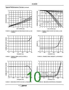
ICL8038
Neither time nor frequency are dependent on supply voltage,
R and R are shown in the Detailed Schematic.
1 2
even though none of the voltages are regulated inside the
integrated circuit. This is due to the fact that both currents
and thresholds are direct, linear functions of the supply
voltage and thus their effects cancel.
A similar calculation holds for R .
B
The capacitor value should be chosen at the upper end of its
possible range.
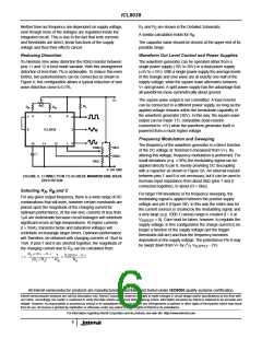
Reducing Distortion
Waveform Out Level Control and Power Supplies
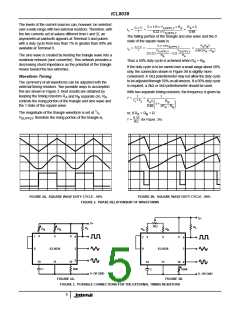
To minimize sine wave distortion the 82kΩ resistor between
pins 11 and 12 is best made variable. With this arrangement
distortion of less than 1% is achievable. To reduce this even
further, two potentiometers can be connected as shown in
Figure 4; this configuration allows a typical reduction of sine
wave distortion close to 0.5%.
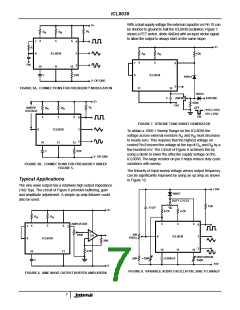
The waveform generator can be operated either from a
single power supply (10V to 30V) or a dual power supply
(±5V to ±15V). With a single power supply the average levels
of the triangle and sine wave are at exactly one-half of the
supply voltage, while the square wave alternates between
V+ and ground. A split power supply has the advantage that
all waveforms move symmetrically about ground.
V+
The square wave output is not committed. A load resistor
can be connected to a different power supply, as long as the
applied voltage remains within the breakdown capability of
the waveform generator (30V). In this way, the square wave
output can be made TTL compatible (load resistor
connected to +5V) while the waveform generator itself is
powered from a much higher voltage.
1kΩ
R
L
R
R
B
A
4
5
6
1
7
9
3
8
ICL8038
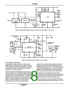
Frequency Modulation and Sweeping
2
10
11
12
The frequency of the waveform generator is a direct function
of the DC voltage at Terminal 8 (measured from V+). By
altering this voltage, frequency modulation is performed. For
small deviations (e.g. ±10%) the modulating signal can be
applied directly to pin 8, merely providing DC decoupling
with a capacitor as shown in Figure 5A. An external resistor
between pins 7 and 8 is not necessary, but it can be used to
increase input impedance from about 8kΩ (pins 7 and 8
connected together), to about (R + 8kΩ).
100kΩ
10kΩ
10kΩ
C
100kΩ
V- OR GND
FIGURE 4. CONNECTION TO ACHIEVE MINIMUM SINE WAVE
DISTORTION
Selecting R , R and C
A
B
For larger FM deviations or for frequency sweeping, the
modulating signal is applied between the positive supply
voltage and pin 8 (Figure 5B). In this way the entire bias for
the current sources is created by the modulating signal, and
a very large (e.g. 1000:1) sweep range is created (f = 0 at
For any given output frequency, there is a wide range of RC
combinations that will work, however certain constraints are
placed upon the magnitude of the charging current for
optimum performance. At the low end, currents of less than
1µA are undesirable because circuit leakages will contribute
significant errors at high temperatures. At higher currents
(I > 5mA), transistor betas and saturation voltages will
contribute increasingly larger errors. Optimum performance
will, therefore, be obtained with charging currents of 10µA to
1mA. If pins 7 and 8 are shorted together, the magnitude of
V
= 0). Care must be taken, however, to regulate the
SWEEP
supply voltage; in this configuration the charge current is no
longer a function of the supply voltage (yet the trigger
thresholds still are) and thus the frequency becomes
dependent on the supply voltage. The potential on Pin 8 may
1
be swept down from V+ by ( / V
- 2V).
SUPPLY
3
the charging current due to R can be calculated from:
A
R
× (V+ – V-)
1
1
0.22(V+ – V-)
---------------------------------------- -------
I =
×
= -----------------------------------
(R + R )
R
R
1
2
A
A
All Intersil semiconductor products are manufactured, assembled and tested under ISO9000 quality systems certification.
Intersil semiconductor products are sold by description only. Intersil Corporation reserves the right to make changes in circuit design and/or specifications at any time with-
out notice. Accordingly, the reader is cautioned to verify that data sheets are current before placing orders. Information furnished by Intersil is believed to be accurate and
reliable. However, no responsibility is assumed by Intersil or its subsidiaries for its use; nor for any infringements of patents or other rights of third parties which may result
from its use. No license is granted by implication or otherwise under any patent or patent rights of Intersil or its subsidiaries.
For information regarding Intersil Corporation and its products, see web site http://www.intersil.com
6

 INTERSIL [ Intersil ]