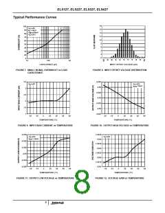
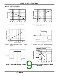
EL5127, EL5227, EL5327, EL5427
application to determine if load conditions need to be
modified for the buffer to remain in the safe operating area.
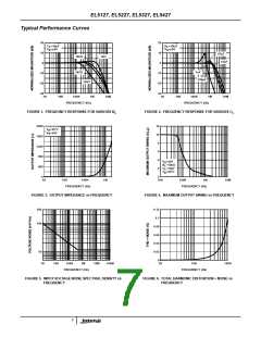
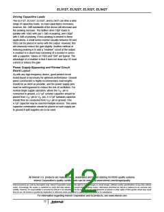
5V
10µs
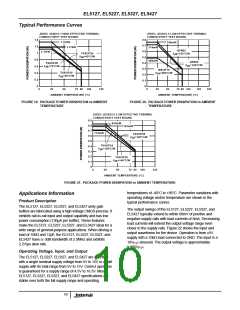
The maximum power dissipation allowed in a package is
determined according to:
T
- T
AMAX
JMAX
P
= --------------------------------------------
DMAX
Θ
JA
V =±5V
S
where:
T =25°C
A
V
=10V
P-P
IN
5V
T
= Maximum junction temperature
= Maximum ambient temperature
JMAX
FIGURE 22. OPERATION WITH RAIL-TO-RAIL INPUT AND
OUTPUT
T
AMAX
Short Circuit Current Limit
θ
= Thermal resistance of the package
JA
The EL5127, EL5227, EL5327, and EL5427 will limit the
short circuit current to ±120mA if the output is directly
shorted to the positive or the negative supply. If an output is
shorted indefinitely, the power dissipation could easily
increase such that the device may be damaged. Maximum
reliability is maintained if the output continuous current never
exceeds ±30mA. This limit is set by the design of the internal
metal interconnects.
P
= Maximum power dissipation in the package
DMAX
The maximum power dissipation actually produced by an IC
is the total quiescent supply current times the total power
supply voltage, plus the power in the IC due to the loads, or:
P
= Σi[V × I
+ (V + - V
i) × I
i]
LOAD
DMAX
S
SMAX
S
OUT
when sourcing, and:
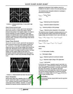
Output Phase Reversal
The EL5127, EL5227, EL5327, and EL5427 are immune to
phase reversal as long as the input voltage is limited from
P
= Σi[V × I
+ (V
i - V -) × I
i]
LOAD
DMAX
S
SMAX
OUT
S
V - -0.5V to V + +0.5V. Figure 23 shows a photo of the
S
S
when sinking.
where:
output of the device with the input voltage driven beyond the
supply rails. Although the device's output will not change
phase, the input's overvoltage should be avoided. If an input
voltage exceeds supply voltage by more than 0.6V,
electrostatic protection diodes placed in the input stage of
the device begin to conduct and overvoltage damage could
occur.
i = 1 to Total number of buffers
V = Total supply voltage
S
I
= Maximum quiescent current per channel
SMAX
1V
10µs
V
i = Maximum output voltage of the application
OUT
I
i = Load current
LOAD
If we set the two P
equations equal to each other, we
i to avoid device overheat. The package
DMAX
can solve for R
LOAD
power dissipation curves provide a convenient way to see if
the device will overheat. The maximum safe power
V =±2.5V
S
T =25°C
A
dissipation can be found graphically, based on the package
type and the ambient temperature. By using the previous
V
=6V
IN
P-P
1V
equation, it is a simple matter to see if P
device's power derating curves.
exceeds the
DMAX
FIGURE 23. OPERATION WITH BEYOND-THE-RAILS INPUT
Unused Buffers
Power Dissipation
It is recommended that any unused buffer have the input tied
to the ground plane.
With the high-output drive capability of the EL5127, EL5227,
EL5327, and EL5427 buffer, it is possible to exceed the
125°C “absolute-maximum junction temperature” under
certain load current conditions. Therefore, it is important to
calculate the maximum junction temperature for the
11

 INTERSIL [ Intersil ]