EL5127, EL5227, EL5327, EL5427
Absolute Maximum Ratings (T = 25°C)
A
Supply Voltage Between V + and V -. . . . . . . . . . . . . . . . . . . .+18V
Maximum Die Temperature . . . . . . . . . . . . . . . . . . . . . . . . . . +125°C
Storage Temperature . . . . . . . . . . . . . . . . . . . . . . . .-65°C to +150°C
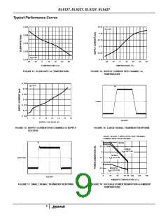
Power Dissipation . . . . . . . . . . . . . . . . . . . . . . . . . . . . . See Curves
Operating Temperature . . . . . . . . . . . . . . . . . . . . . . .-40°C to +85°C
S
S
Input Voltage . . . . . . . . . . . . . . . . . . . . . . . . . . .V - -0.5V, V +0.5V
S
S
Maximum Continuous Output Current . . . . . . . . . . . . . . . . . . . 30mA
ESD Voltage. . . . . . . . . . . . . . . . . . . . . . . . . . . . . . . . . . . . . . . . .2kV
CAUTION: Stresses above those listed in “Absolute Maximum Ratings” may cause permanent damage to the device. This is a stress only rating and operation of the
device at these or any other conditions above those indicated in the operational sections of this specification is not implied.
IMPORTANT NOTE: All parameters having Min/Max specifications are guaranteed. Typ values are for information purposes only. Unless otherwise noted, all tests are
at the specified temperature and are pulsed tests, therefore: T = T = T
A
J
C
Electrical Specifications V + = +5V, V - = -5V, R = 10kΩ, C = 10pF to 0V, T = 25°C, unless otherwise specified.
S
S
L
L
A
PARAMETER
DESCRIPTION
CONDITIONS
MIN
TYP
MAX
15
UNIT
INPUT CHARACTERISTICS
V
Input Offset Voltage
V
= 0V
1
5
mV
µV/°C
nA
OS
TCV
CM
(Note 1)
= 0V
Average Offset Voltage Drift
Input Bias Current
Input Impedance
OS
I
V
2
50
B
CM
R
1
GΩ
IN
IN
C
Input Capacitance
Voltage Gain
1.35
pF
AV
-4.5V ≤ V
≤ 4.5V
0.99
1.01
-4.85
30
V/V
OUT
OUTPUT CHARACTERISTICS
V
V
Output Swing Low
I = -5mA
-4.95
4.95
V
V
OL
OH
L
Output Swing High
I = +5mA
4.85
100
L
I
(max)
Max Output Current (Note 2)
R
= 10Ω
±120
mA
OUT
L
POWER SUPPLY PERFORMANCE
PSRR Power Supply Rejection Ratio
Supply Current
V
is moved from ±2.25V to ±7.75V
55
80
0.7
1.2
1.4
1.6
dB
mA
mA
mA
mA
S
I
No load (EL5127)
No load (EL5227)
No load (EL5327)
No load (EL5427)
0.9
1.4
2
S
2.2
DYNAMIC PERFORMANCE
SR Slew Rate (Note 3)
-4.0V ≤ V
≤ 4.0V, 20% to 80%
0.9
2.2
900
2.5
75
V/µs
ns
OUT
(A = +1), V = 2V step
t
Settling to +0.1% (A = +1)
V
S
V
O
BW
-3dB Bandwidth
R
= 10kΩ, C = 10pF
MHz
dB
L
L
CS
Channel Separation
f = 100kHz
NOTES:
1. Measured over operating temperature range.
2. Instantaneous peak current.
3. Slew rate is measured on rising and falling edges.
4

 INTERSIL [ Intersil ]