EL5127, EL5227, EL5327, EL5427
Typical Performance Curves
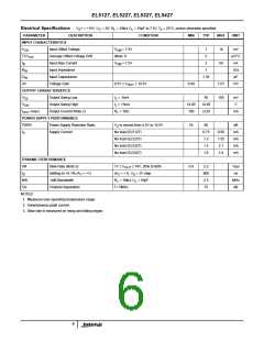
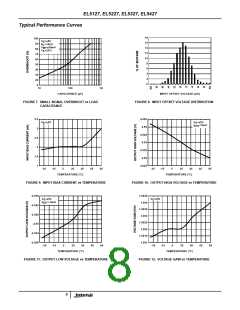
JEDEC JESD51-7 HIGH EFFECTIVE THERMAL
JEDEC JESD51-3 LOW EFFECTIVE THERMAL
CONDUCTIVITY TEST BOARD
CONDUCTIVITY TEST BOARD
758mW
1.4
1.2
1
0.8
0.7
0.6
0.5
0.4
0.3
0.2
0.1
0
1.333W
1.176W
714mW
QFN32
1.111W
TSSOP24
=85°C/W
θ
=132°C/W
JA
θ
JA
0.8
0.6
0.4
0.2
0
486mW
QFN24
=140°C/W
TSSOP28
θ
JA
θ
=75°C/W
JA
MSOP10
TSSOP20
=90°C/W
θ
=206°C/W
JA
θ
JA
0
25
50
75 85 100
125
0
25
50
75 85 100
125
150
AMBIENT TEMPERATURE (°C)
AMBIENT TEMPERATURE (°C)
FIGURE 19. PACKAGE POWER DISSIPATION vs AMBIENT
TEMPERATURE
FIGURE 20. PACKAGE POWER DISSIPATION vs AMBIENT
TEMPERATURE
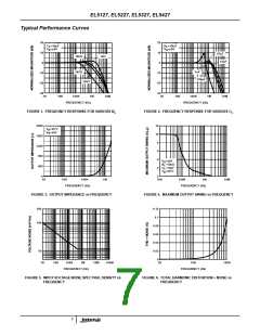
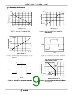
JEDEC JESD51-3 LOW EFFECTIVE THERMAL
CONDUCTIVITY TEST BOARD
0.9
0.8
0.7
0.6
0.5
0.4
0.3
0.2
0.1
0
833mW
781mW
714mW
TSSOP28
=120°C/W
θ
JA
TSSOP24
=128°C/W
θ
JA
TSSOP20
=140°C/W
θ
JA
0
25
50
75 85 100
125
AMBIENT TEMPERATURE (°C)
FIGURE 21. PACKAGE POWER DISSIPATION vs AMBIENT TEMPERATURE
temperatures of -40°C to +85°C. Parameter variations with
operating voltage and/or temperature are shown in the
typical performance curves.
Applications Information
Product Description
The EL5127, EL5227, EL5327, and EL5427 unity gain
buffers are fabricated using a high voltage CMOS process. It
exhibits rail-to-rail input and output capability and has low
power consumption (120µA per buffer). These features
make the EL5127, EL5227, EL5327, and EL5427 ideal for a
wide range of general-purpose applications. When driving a
load of 10kΩ and 12pF, the EL5127, EL5227, EL5327, and
EL5427 have a -3dB bandwidth of 2.5MHz and exhibits
2.2V/µs slew rate.
The output swings of the EL5127, EL5227, EL5327, and
EL5427 typically extend to within 80mV of positive and
negative supply rails with load currents of 5mA. Decreasing
load currents will extend the output voltage range even
closer to the supply rails. Figure 22 shows the input and
output waveforms for the device. Operation is from ±5V
supply with a 10kΩ load connected to GND. The input is a
10V
sinusoid. The output voltage is approximately
P-P
9.985V
.
P-P
Operating Voltage, Input, and Output
The EL5127, EL5227, EL5327, and EL5427 are specified
with a single nominal supply voltage from 5V to 15V or a split
supply with its total range from 5V to 15V. Correct operation
is guaranteed for a supply range of 4.5V to 16.5V. Most
EL5127, EL5227, EL5327, and EL5427 specifications are
stable over both the full supply range and operating
10

 INTERSIL [ Intersil ]