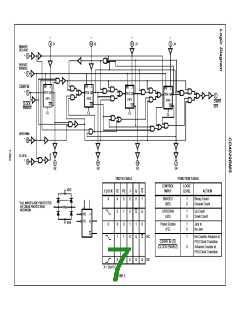
CD4029BMS
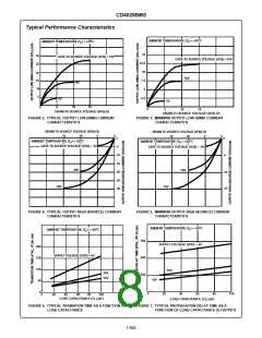
Typical Performance Characteristics (Continued)
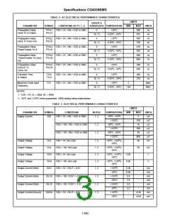
105
8
6
AMBIENT TEMPERATURE (TA) = +25oC
4
SUPPLY VOLTAGE (VDD) = 15V
10V
2
104
SUPPLY VOLTAGE (VDD) = 5V
8
6
300
200
100
4
2
103
102
10
8
6
10V
5V
4
2
10V
8
6
4
CL = 50pF
CL = 15pF
15V
2
AMBIENT TEMPERATURE (TA) = +25oC
2
4
6 8
2
4
6 8
2
4
6 8
103
2
4
6 8
2
4 6 8
0
20
40
60
80
100
102
104
1
10
CLOCKFREQUENCY (fCL) (kHz)
LOAD CAPACITANCE (CL) (pF)
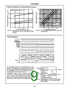
FIGURE 8. TYPICAL PROPAGATION DELAY TIME AS A
FIGURE 9. TYPICAL POWER DISSIPATION AS A FUNCTION
OF FREQUENCY
FUNCTION OF LOAD CAPACITANCE (CARRY
OUTPUT)
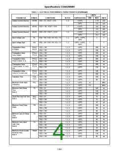
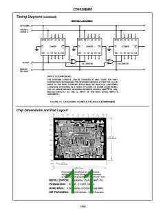
Timing Diagrams
CLOCK (CL)
CARRY IN
(CL ENABLE)
UP/DOWN
BINARY/
DECADE
PRESET
ENABLE
J1
J2
J3
J4
Q1
Q2
Q3
Q4
CARRY OUT
COUNT
5
6
7
8
9
10 11 12 13 14 15
9
8
7
6
5
4
3
2
1
0
0
15
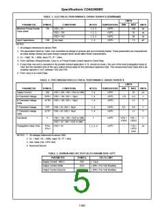
The CD4029BMS CLOCK and UP/DOWN inputs are used
directly in most applications. In applications where CLOCK
UP and CLOCK DOWN inputs are provided, conversion to
the CD4029BMS CLOCK and UP/DOWN inputs can easily
be realized by use of the circuit in Figure 11.
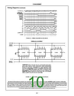
“CLOCK UP”
“UP/DOWN”
“CLOCK”
VDD
“CLOCK
DOWN”
CD4029BMS changes count on positive transitions of
CLOCK UP or CLOCK DOWN inputs. For the gate configu-
ration in Figure 12, when counting up the CLOCK DOWN
input must be maintained high and conversely when count-
ing down the CLOCK UP input must be maintained high.
1 CD4011
QUAD 2 INPUT NAND GATE
FIGURE 11. CONVERSION OF CLOCK UP, CLOCK DOWN
INPUT SIGNALS TO CLOCK AND UP/DOWN
INPUT SIGNALS
7-806

 INTERSIL [ Intersil ]