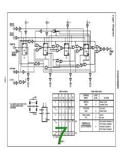
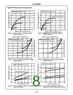
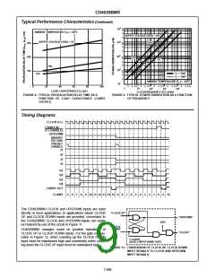
Specifications CD4029BMS
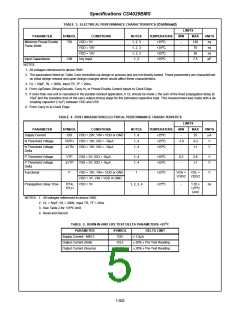
TABLE 3. ELECTRICAL PERFORMANCE CHARACTERISTICS (Continued)
LIMITS
PARAMETER
SYMBOL
CONDITIONS
VDD = 5V
NOTES
1, 2, 3
1, 2, 3
1, 2, 3
1, 2
TEMPERATURE
MIN
MAX
130
70
UNITS
ns
o
Minimum Preset Enable
Pulse Width
TW
+25 C
-
-
-
-
o
VDD = 10V
VDD = 15V
Any Input
+25 C
ns
o
+25 C
50
ns
o
Input Capacitance
NOTES:
CIN
+25 C
7.5
pF
1. All voltages referenced to device GND.
2. The parameters listed on Table 3 are controlled via design or process and are not directly tested. These parameters are characterized
on initial design release and upon design changes which would affect these characteristics.
3. CL = 50pF, RL = 200K, Input TR, TF < 20ns.
4. From Up/Down, Binary/Decode, Carry In, or Preset Enable Control Inputs to Clock Edge.
5. If more than one unit is cascaded in the parallel clocked application, tr CL should be made ≤ the sum of the fixed propagation delay at
15pF and the transition time of the carry output driving stage for the estimated capacitive load. This measurement was made with a de-
coupling capacitor (>1µF) between VDD and VSS.
6. From Carry In to Clock Edge.
TABLE 4. POST IRRADIATION ELECTRICAL PERFORMANCE CHARACTERISTICS
LIMITS
PARAMETER
Supply Current
SYMBOL
IDD
CONDITIONS
NOTES
1, 4
TEMPERATURE
MIN
MAX
25
UNITS
o
VDD = 20V, VIN = VDD or GND
VDD = 10V, ISS = -10µA
VDD = 10V, ISS = -10µA
+25 C
-
-2.8
-
µA
V
o
N Threshold Voltage
VNTH
∆VTN
1, 4
+25 C
-0.2
±1
o
N Threshold Voltage
Delta
1, 4
+25 C
V
o
P Threshold Voltage
VTP
VSS = 0V, IDD = 10µA
VSS = 0V, IDD = 10µA
1, 4
1, 4
+25 C
0.2
-
2.8
V
V
o
P Threshold Voltage
Delta
∆VTP
+25 C
±1
o
Functional
F
VDD = 18V, VIN = VDD or GND
VDD = 3V, VIN = VDD or GND
VDD = 5V
1
+25 C
VOH >
VDD/2
VOL <
VDD/2
V
o
Propagation Delay Time
TPHL
TPLH
1, 2, 3, 4
+25 C
-
1.35 x
ns
o
+25 C
Limit
NOTES: 1. All voltages referenced to device GND.
2. CL = 50pF, RL = 200K, Input TR, TF < 20ns
o
3. See Table 2 for +25 C limit.
4. Read and Record
O
TABLE 5. BURN-IN AND LIFE TEST DELTA PARAMETERS +25 C
PARAMETER
Supply Current - MSI-2
Output Current (Sink)
Output Current (Source)
SYMBOL
IDD
DELTA LIMIT
± 1.0µA
IOL5
± 20% x Pre-Test Reading
± 20% x Pre-Test Reading
IOH5A
7-802

 INTERSIL [ Intersil ]