BBT3821
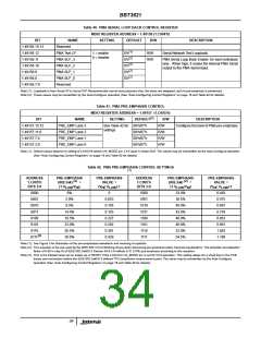
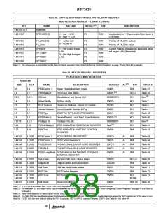
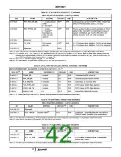
Table 55. OPTICAL STATUS & CONTROL PIN POLARITY REGISTER
MDIO REGISTER ADDRESS = 1.49181 (1.C01D’h)
(1)
BIT
1.49181.15:7
1.49181.6
NAME
Reserved
SETTING
DEFAULT
R/W
DESCRIPTION
OPRLOS[3:0]
1 = low -> LOS
0 = high -> LOS
0’b
R/W
Input polarity to 1.10 and enable Byte Synch in
LX4 mode
1.49181.5
1.49181.4
1.49181.3
1.49181.2
1.49181.1
1.49181.0
TX_ENA[3:0]
TX_ENC
1 = Active Low
0 = Active Hi
0’b
0’b
0’b
0’b
0’b
0’b
R/W
R/W
R/W
R/W
R/W
R/W
Polarity of TX_ENA outputs
Polarity of TX_ENC input
OPRXOP
1 = Pin Low to trigger
LASI
0 = Pin High to trigger
LASI
Control Polarity of respective input pins which
will trigger LASI (if enabled)
OPTTEMP
OPTXLBC
OPTXLOP
Note (1): The values may be overwritten by the Auto-Configure operation (See “Auto-Configuring Control Registers” on page 16 and Table 92 for details).
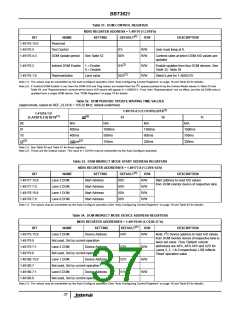
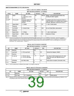
Table 56. MDIO PCS DEVAD 3 REGISTERS
PCS DEVICE 3 MDIO REGISTERS
ADDRESS
DEC HEX
3.0
(2)
NAME
PCS Control 1
PCS Status 1
ID Code
DESCRIPTION
Reset, Enable loop back mode.
PCS Fault, Link Status
DEFAULT
2040’h
AC
R/W
R/W
DETAILS
Table 57
3.0
3.1
(3)
3.1
0004’h
RO LL
RO
Table 58
(1)
3.2:3
3.4
3.2:3
3.4
Manufacturer and Device OUI
10Gbps Ability
01839C6V’h
0001’h
See
Speed Ability
IEEE Devices
RO
Table 7
Table 8
Table 8
Table 59
Table 60
3.5
3.5
Devices in Package, Clause 22 capable
001A’h
RO
3.6
3.6
Vendor Devices Vendor Specific Devices in Pkg
0000’h
RO
3.7
3.7
PCS Type
IEEE PCS TYPE SELECT REGISTER
Device Present, Local Fault, Type Summary
Package OUI, etc.
0001’h
RO
(3)
3.8
3.8
PCS Status 2
Package ID
PCS-X Status 3
PCS Test
8002’h
RO
(4)
3.14:15
3.24
3.25
3.E:F
3.18
3.19
00000000’h
RO
See
(5)
IEEE 10GBASE-X PCS STATUS REGISTER
See
RO
Table 61
Table 62
IEEE 10GBASE-X PCS TEST CONTROL
REGISTER
0000’h
R/W
3.49152
3.49153
3.49154
3.49155
3.49156
3.C000
3.C001
3.C002
3.C003
3.C004
PCS Control 2
PCS Control 3
PCS ERROR
PCS IDLE
PCS CONTROL REGISTER 2
0F6F’h
0801’h
00FE’h
0007’h
0000’h
A
A
A
A
A
R/W
R/W
R/W
R/W
R/W
Table 63
Table 64
Table 66
Table 67
Table 68
PCS Control Register 3
PCS INTERNAL ERROR CODE REGISTER
PCS INTERNAL IDLE CODE REGISTER
PCS // Loop Back PCS PARALLEL NETWORK LOOP BACK
CONTROL REGISTER
3.49159
3.49160
3.49161
3.49164
3.C007
3.C008
3.C009
3.C00C
Test_Flags
Output Ctrl
Half Rate
BIST Ctrl
Receive Path Test & Status Flags
Output Control and Test function
Half rate clock mode enable
BIST Control Register
0000’h
AAAA’h
0000’h
0000’h
0000’h
RO LH
R/W
Table 69
Table 70
Table 71
Table 72
Table 73
R/W
R/W
3.49165
3.49166
3.C00D
3.C00E
BIST Error
BIST ERROR Counter Registers
RO/
RCNR
3.49167
3.C00F
Soft Reset
Reset (non MDIO)
0000’h
R/W SC
Table 46
Note (1): ‘V’ is a version number. See “JTAG & AC-JTAG Operations” on page 53 for a note about the version number.
Note (2): For rows with “A”, the default value may be overwritten by the Auto-Configure operation (See “Auto-Configuring Control Registers” on page 16 and Table 92
for details).
Note (3): Read value depends on status signal values. Value shown indicates ‘normal’ operation.
Note (4): The IEEE 802.3ae specification allows this to be all zeroes. A XENPAK (etc.) host can more readily determine where the NVR registers are if this value is zero.
Note (5): If IEEE 802.3ae (and default) setting for PCS Loopback, 180F’h. If PCS Loopback allowed, 1C0F’h. See Table 61 and Table 64.
38

 INTERSIL [ Intersil ]