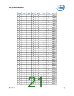
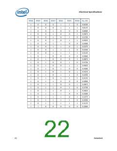
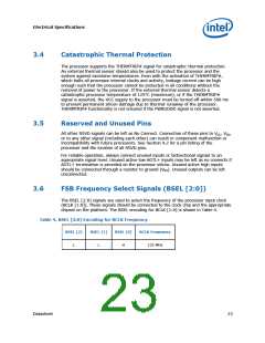
Electrical Specifications
3.7
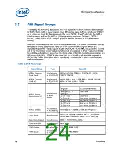
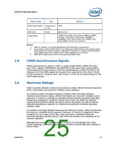
FSB Signal Groups
To simplify the following discussion, the FSB signals have been combined into groups
by buffer type. AGTL+ input signals have differential input buffers, which use GTLREF
as a reference level. In this document, the term “AGTL+ Input” refers to the AGTL+
input group as well as the AGTL+ I/O group when receiving. Similarly, “AGTL+
Output” refers to the AGTL+ output group as well as the AGTL+ I/O group when
driving.
With the implementation of a source synchronous data bus comes the need to specify
two sets of timing parameters. One set is for common clock signals which are
dependent upon the rising edge of BCLK0 (ADS#, HIT#, HITM#, etc.) and the second
set is for the source synchronous signals which are relative to their respective strobe
lines (data and address) as well as the rising edge of BCLK0. Asynchronous signals are
still present (A20M#, IGNNE#, etc.) and can become active at any time during the
clock cycle. Table 5 identifies which signals are common clock, source synchronous,
and asynchronous.
Table 5. FSB Pin Groups
Signal Group
Type
Signals1
AGTL+ Common
Clock Input
Synchronous
to BCLK [1:0]
BPRI#, DEFER#, PREQ#4, RESET#, RS [2:0]#,
TRDY#, DPWR#
AGTL+ Common
Clock I/O
Synchronous
to BCLK [1:0]
ADS#, BNR#, BPM [3:0]#, BR0#, DBSY#, DRDY#,
HIT#, HITM#, LOCK#, PRDY#
Signals
Associated Strobe
REQ [4:0]#, A
[16:3]#
ADSTB0#
Synchronous
to assoc.
strobe
AGTL+ Source
Synchronous I/O
A [31:17]#
D [15:0]#
D [31:16]#
D [47:32]#
D [63:48]#
ADSTB1#
DSTBP0#, DSTBN0#
DSTBP1#, DSTBN1#
DSTBP2#, DSTBN2#
DSTBP3#, DSTBN3#
Synchronous
to BCLK [1:0]
AGTL+ Strobes
CMOS Input
ADSTB [1:0]#, DSTBP [3:0]#, DSTBN [3:0]#
DPRSTP#, DPSLP#, IGNNE#, INIT#, LINT0/INTR,
LINT1/ NMI, PWRGOOD, SMI#, SLP#, STPCLK#
Asynchronous
Open Drain Output
Open Drain I/O
CMOS Output
Asynchronous
Asynchronous
Asynchronous
FERR#, THERMTRIP#, IERR#
PROCHOT#3
VID [6:0], BSEL [2:0]
Synchronous
to TCK
CMOS Input
TCK, TDI, TMS, TRST#
24
Datasheet

 INTEL [ INTEL ]