Electrical Specifications
3
Electrical Specifications
3.1
Power and Ground Pins
For clean, on-chip power distribution, the processor will have a large number of VCC
(power) and VSS (ground) inputs. All power pins must be connected to VCC power
planes while all VSS pins must be connected to system ground planes. Use of multiple
power and ground planes is recommended to reduce I*R drop. The processor VCC pins
must be supplied the voltage determined by the VID (Voltage ID) pins.
3.2
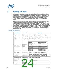
3.3
FSB Clock (BCLK [1:0]) and Processor Clocking
BCLK [1:0] directly controls the FSB interface speed as well as the core frequency of
the processor. As in previous generation processors, the processor core frequency is a
multiple of the BCLK [1:0] frequency. The processor uses a differential clocking
implementation.
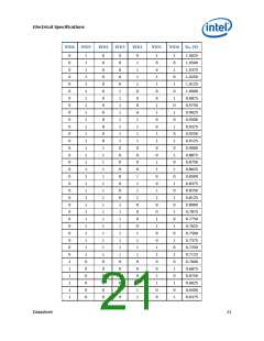
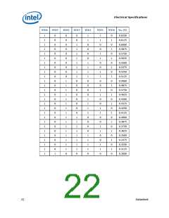
Voltage Identification
The processor uses seven voltage identification pins (VID [6:0]) to support automatic
selection of power supply voltages. The VID pins for the processor are CMOS outputs
driven by the processor VID circuitry. Table 3 specifies the voltage level corresponding
to the state of VID [6:0]. A “1” in this refers to a high-voltage level and a “0” refers to
low-voltage level.
Table 3. Voltage Identification Definition
VID6
VID5
VID4
VID3
VID2
VID1
VID0
VCC (V)
0
0
0
0
0
0
0
0
0
0
0
0
0
0
0
0
0
0
0
1
1
1
1
1
1
1
1
1
1
1
0
0
0
1
1
1
1
1
1
1
1
0
0
0
0
0
0
0
1
1
1
1
0
0
0
0
0
1
1
0
0
1
1
0
0
1
0
1
0
1
0
1
0
1
0
1
0
1.2000
1.1875
1.1750
1.1625
1.1500
1.1375
1.1250
1.1125
1.1000
1.0875
1.0750
20
Datasheet

 INTEL [ INTEL ]