LXT971A 3.3 V Dual-Speed Fast Ethernet Transceiver
Revision History
Revision 002
Revision Date: August 6, 2002
Page
Description
Globally replaced “pseudo-PECL” with Low-Voltage PECL”, except when identified with 5 V.
Front Page: Changed “pseudo-ECL (PECL)” to “Low Voltage PECL (LVPECL).
Added “JTAG Boundary Scan” to Product Features on front page.
1
12
13
14
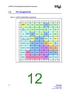
Modified Figure 2 “LXT971A 64-Ball PBGA Assignments” (replaced TEST1 and TEST0 with GND).
Modified Figure 3 “LXT971A 64-Pin LQFP Assignments” (replaced TEST1 and TEST0 with GND).
Modified Table 1 “LQFP Numeric Pin List” (replaced TEST1 and TEST0 with GND).
Added note under Section 2.0, “Signal Descriptions”: “Intel recommends that all inputs and multi-
function pins be tied to the inactive states and all outputs be left floating, if unused.”
16
17
Modified SD/TP description in Table 3 “LXT971A Network Interface Signal Descriptions”.
Added Table note 2.
18
19
20
22
23
Modified Table 4 “LXT971A Miscellaneous Signal Descriptions”.
Modified Table 5 “LXT971A Power Supply Signal Descriptions”.
Added Table 8 “LXT971A Pin Types and Modes”.
Replaced second paragraph under Section 3.2.1.2, “Fiber Interface”.
Added Section 3.2.2.1, “Increased MII Drive Strength”.
Changed “Far-End Fault” title to ‘100BASE-FX Far-End Fault”.
Modified first sentence under this heading.
23
30
35
43
47
47
52
53
54
55
56
56
57
58
58
60
65
72
86
87
90
Modified Figure 8 “Hardware Configuration Settings”.
Added paragraph after bullets under Section 3.6.7.2, “Test Loopback”.
Modified text under Section 3.7.3.4, “Fiber PMD Sublayer”.
Modified Table 13 “Supported JTAG Instructions”.
Modified Table 14 “Device ID Register”.
Added a new Section 4.3, “The Fiber Interface”.
Replaced Figure 25 “Typical LXT971A-to-3.3 V Fiber Transceiver Interface Circuitry”.
Added Figure 26 “Typical LXT971A-to-5 V Fiber Transceiver Interface Circuitry”.
Added Figure 27 “ON Semiconductor Triple PECL-to-LVPECL Translator”.
Modified Table 17 “Absolute Maximum Ratings”.
Modified Table 18 “Operating Conditions”: Added Typ values to Vcc current.
Modified Table 20 “Digital I/O Characteristics - MII Pins”.
Modified Table 22 “I/O Characteristics - LED/CFG Pins”.
Added Table 23 “I/O Characteristics – SD/TP Pin”.
Added Table 28 “LXT971A Thermal Characteristics”.
Modified Table 33 “10BASE-T Receive Timing Parameters”
Modified Table 42 “Register Bit Map”. (Added Table 26 information).
Added Table 57 “Digital Config Register (Address 26)”.
Modified Table 58 “Transmit Control Register (Address 30)”.
Added Section 8.0, “Product Ordering Information”.
8
Datasheet
Document #: 249414
Revision #: 002
Rev. Date: August 7, 2002

 INTEL [ INTEL ]