LXT971A 3.3V Dual-Speed Fast Ethernet Transceiver
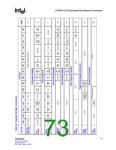
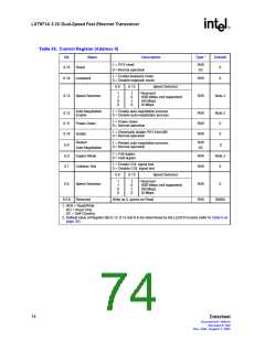
Table 43. Control Register (Address 0)
Bit
Name
Description
Type 1
Default
1 = PHY reset
0 = Normal operation
R/W
SC
0.15
Reset
0
1 = Enable loopback mode
0 = Disable loopback mode
0.14
Loopback
R/W
0
0.6
0.13
Speed Selected
1
1
0
0
1
0
1
0
Reserved
0.13
Speed Selection
R/W
Note 2
1000 Mbps (not supported)
100 Mbps
10 Mbps
Auto-Negotiation
Enable
1 = Enable auto-negotiation process
0 = Disable auto-negotiation process
0.12
0.11
0.10
R/W
R/W
R/W
Note 2
1 = Power-down
Power-Down
Isolate
0
0
0 = Normal operation
1 = Electrically isolate PHY from MII
0 = Normal operation
Restart
Auto-Negotiation
R/W
SC
1 = Restart auto-negotiation process
0 = Normal operation
0.9
0
1 = Full-duplex
0 = Half-duplex
0.8
0.7
Duplex Mode
Collision Test
R/W
R/W
Note 2
0
1 = Enable COL signal test
0 = Disable COL signal test
0.6
0.13
Speed Selected
1
1
0
0
1
0
1
0
Reserved
0.6
Speed Selection
Reserved
R/W
R/W
0
1000 Mbps (not supported)
100 Mbps
10 Mbps
0.5:0
Write as 0, ignore on Read
00000
1. R/W = Read/Write
RO = Read Only
SC = Self Clearing
2. Default value of Register bits 0.12, 0.13 and 0.8 are determined by the LED/CFGn pins (refer to Table 9 on
page 30).
74
Datasheet
Document #: 249414
Revision #: 002
Rev. Date: August 7, 2002

 INTEL [ INTEL ]