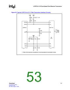
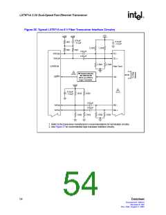
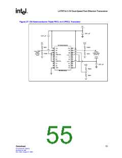
LXT971A 3.3V Dual-Speed Fast Ethernet Transceiver
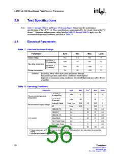
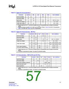
Table 19. Digital I/O Characteristics2
1
Parameter
Symbol
Min
Typ
Max
Units
Test Conditions
Input Low voltage
Input High voltage
Input current
VIL
VIH
II
–
–
–
–
–
–
0.8
–
V
V
–
2.0
-10
–
–
10
0.4
–
µA
V
0.0 < VI < VCC
IOL = 4 mA
IOH = -4 mA
Output Low voltage
Output High voltage
VOL
VOH
2.4
V
1. Typical values are at 25 °C and are for design aid only; not guaranteed and not subject to production
testing.
2. Applies to all pins except MII, LED, XI/XO, and SD/TP pins. Refer to Table 20 for MII I/O Characteristics,
Table 21 for XI/XO and Table 22 for LED Characteristics.
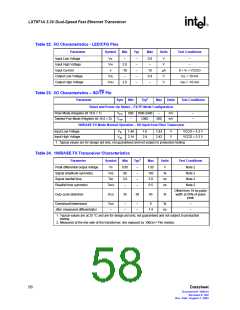
Table 20. Digital I/O Characteristics - MII Pins
1
Parameter
Input Low voltage
Symbol
Min
Typ
Max
Units
Test Conditions
VIL
VIH
II
–
2.0
-10
–
–
–
0.8
–
V
V
–
Input High voltage
Input current
–
–
10
0.4
–
µA
V
0.0 < VI < VCCIO
IOL = 4 mA
Output Low voltage
VOL
VOH
VOH
–
2.2
2.0
–
–
V
IOH = -4 mA, VCCIO = 3.3V
IOH = -4 mA, VCCIO = 2.5V
VCCIO = 2.5V
Output High voltage
–
–
V
2
RO
100
100
–
W
W
Driver output resistance
2
(Line driver output enabled)
RO
–
–
VCCIO = 3.3V
1. Typical values are at 25 °C and are for design aid only; not guaranteed and not subject to production
testing.
2. Parameter is guaranteed by design; not subject to production testing.
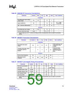
Table 21. I/O Characteristics - REFCLK/XI and XO Pins
Parameter
Input Low Voltage
Symbol
Min
Typ1
Max
Units
Test Conditions
VIL
VIH
∆f
–
2.0
–
–
–
0.8
–
V
V
–
–
–
–
–
Input High Voltage
Input Clock Frequency Tolerance2
Input Clock Duty Cycle2
Input Capacitance
–
±100
65
ppm
%
Tdc
CIN
35
–
–
3.0
–
pF
1. Typical values are at 25 °C and are for design aid only; not guaranteed and not subject to production
testing.
2. Parameter is guaranteed by design; not subject to production testing.
Datasheet
57
Document #: 249414
Revision #: 002
Rev. Date: August 7, 2002

 INTEL [ INTEL ]