LXT971A 3.3V Dual-Speed Fast Ethernet Transceiver
bit 26.11 through software control. Setting Register bit 26.11 = 1 through the MDC/MDIO
interface sets the MII pins (RXD[0:3], RX_DV, RX_CLK, RX_ER, COL, CRS, and TX_CLK) to a
higher drive strength.
3.2.3
Configuration Management Interface
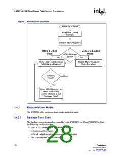
The LXT971A provides both an MDIO interface and a Hardware Control Interface for device
configuration and management.
3.2.3.1
MDIO Management Interface
The LXT971A supports the IEEE 802.3 MII Management Interface also known as the
Management Data Input/Output (MDIO) Interface. This interface allows upper-layer devices to
monitor and control the state of the LXT971A. The MDIO interface consists of a physical
connection, a specific protocol that runs across the connection, and an internal set of addressable
registers.
Some registers are required and their functions are defined by the IEEE 802.3 standard. The
LXT971A also supports additional registers for expanded functionality. The LXT971A supports
multiple internal registers, each of which is 16 bits wide. Specific register bits are referenced using
an “X.Y” notation, where X is the register number (0-31) and Y is the bit number (0-15).
The physical interface consists of a data line (MDIO) and clock line (MDC). Operation of this
interface is controlled by the MDDIS input pin. When MDDIS is High, the MDIO read and write
operations are disabled and the Hardware Control Interface provides primary configuration control.
When MDDIS is Low, the MDIO port is enabled for both read and write operations and the
Hardware Control Interface is not used.
3.2.3.1.1 MDIO Addressing
The protocol allows one controller to communicate with multiple LXT971A chips. Pins
ADDR<4:0> determine the chip address.
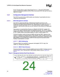
3.2.3.1.2 MDIO Frame Structure
The physical interface consists of a data line (MDIO) and clock line (MDC). The frame structure is
shown in Figures 4 and 5 (read and write). MDIO Interface timing is shown in Table 38 on
page 69.
Figure 4. Management Interface Read Frame Structure
MDC
MDIO
D1
D0
A4
A3
A0
R4
R3
R0
D15 D14
D14 D1
D15
Z
0
32 "1"s
0
1
1
0
(Read)
Turn
Around
Data
Read
Idle
Preamble
ST
Op Code
PHY Address
Register Address
High Z
Write
24
Datasheet
Document #: 249414
Revision #: 002
Rev. Date: August 7, 2002

 INTEL [ INTEL ]