LXT971A 3.3V Dual-Speed Fast Ethernet Transceiver
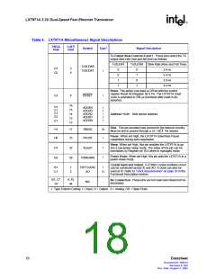
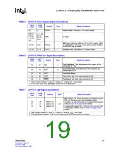
Table 5. LXT971A Power Supply Signal Descriptions
PBGA
Pin#
LQFP
Pin#
Symbol
VCCD
Type
Signal Description
A6
51
–
Digital Power. Requires a 3.3V power supply.
D4, E3
E4, F3
F4, C6,
C3, G7,
G8
7, 11, 18,
25, 34,
35, 41,
50, 61
GND
–
Ground.
MII Power. Requires either a 3.3V or a 2.5V supply. Must
be supplied from the same source used to power the MAC
on the other side of the MII.
E5, D5
G3, G4
8, 40
VCCIO
VCCA
–
–
21, 22
Analog Power. Requires a 3.3V power supply.
Table 6. LXT971A JTAG Test Signal Descriptions
PBGA
Pin#
LQFP
Pin#
Symbol
TDI2
Type1
Signal Description
Test Data Input. Test data sampled with respect to the
F5
27
28
I
rising edge of TCK.
Test Data Output. Test data driven with respect to the
G5
TDO2
O
falling edge of TCK.
F6
G6
H6
29
30
31
TMS2
TCK2
TRST2
I
I
I
Test Mode Select.
Test Clock. Test clock input sourced by ATE.
Test Reset. Test reset input sourced by ATE.
1. Type Column Coding: I = Input, O = Output, A = Analog, OD = Open Drain.
2. If JTAG port is not used, these pins do not need to be terminated.
Table 7. LXT971A LED Signal Descriptions
PBGA
LQFP
Symbol
Type1
Signal Description
Pin#
Pin#
LED Drivers 1-3. These pins drive LED indicators. Each
LED can display one of several available status
conditions as selected by the LED Configuration Register
(refer to Table 56 on page 85 for details).
Configuration Inputs 1-3. These pins also provide initial
configuration settings (refer to Table 9 on page 30 for
details).
E6
F7
F8
38
37
36
LED/CFG1
LED/CFG2
LED/CFG3
I/O
1. Type Column Coding: I = Input, O = Output, A = Analog, OD = Open Drain.
2. Pull-up/pull-down resistors of 10 k can be implemented if LEDs are used in the design.
Datasheet
19
Document #: 249414
Revision #: 002
Rev. Date: August 7, 2002

 INTEL [ INTEL ]