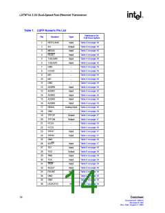
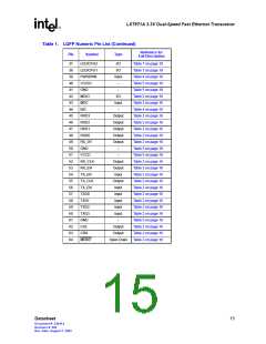
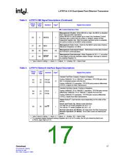
LXT971A 3.3V Dual-Speed Fast Ethernet Transceiver
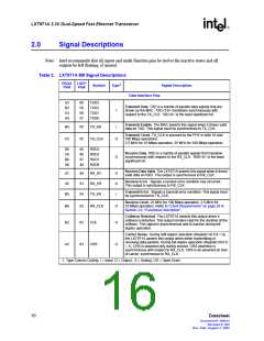
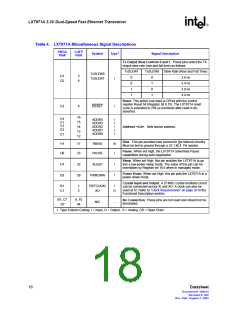
Table 4. LXT971A Miscellaneous Signal Descriptions
PBGA
Pin#
LQFP
Pin#
Symbol
Type1
Signal Description
Tx Output Slew Controls 0 and 1. These pins select the TX
output slew rate (rise and fall time) as follows:
TxSLEW1
TxSLEW0
Slew Rate (Rise and Fall Time)
TxSLEW0
TxSLEW1
D1
D2
5
6
0
0
1
1
0
1
0
1
3.0 ns
3.4 ns
3.9 ns
4.4 ns
I
Reset. This active Low input is OR’ed with the control
register Reset bit (Register bit 0.15). The LXT971A reset
cycle is extended to 258 µs (nominal) after reset is de-
asserted.
C2
4
RESET
I
16
15
14
13
12
G1
F1
F2
E2
E1
H1
H8
ADDR4
ADDR3
ADDR2
ADDR1
ADDR0
I
I
I
I
I
Address <4:0>. Sets device address.
Bias. This pin provides bias current for the internal circuitry.
Must be tied to ground through a 22.1 kΩ, 1% resistor.
17
33
RBIAS
AI
I
Pause. When set High, the LXT971A advertises Pause
PAUSE
capabilities during auto-negotiation.
Sleep. When set High, this pin enables the LXT971A to go
into a low-power sleep mode. The value of this pin can be
overridden by Register bit 16.6 when in managed mode.
H7
E8
32
39
SLEEP
I
I
Power Down. When set High, this pin puts the LXT971A in a
PWRDWN
power-down mode.
Crystal Input and Output. A 25 MHz crystal oscillator circuit
can be connected across XI and XO. A clock can also be
used at XI. Refer to “Clock Requirements” on page 26 in the
Functional Description section.
B1
C1
1
2
REFCLK/XI
XO
I
O
B7, C7
D7
9, 10
44
No Connection. These pins are not used and should not be
N/C
-
terminated.
1. Type Column Coding: I = Input, O = Output, A = Analog, OD = Open Drain.
18
Datasheet
Document #: 249414
Revision #: 002
Rev. Date: August 7, 2002

 INTEL [ INTEL ]