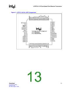
LXT971A 3.3V Dual-Speed Fast Ethernet Transceiver
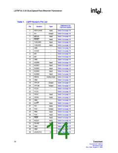
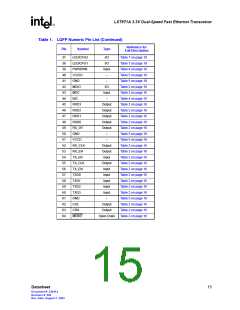
Table 2. LXT971A MII Signal Descriptions (Continued)
PBGA LQFP
Symbol
Type1
Signal Description
Pin#
Pin#
MII Control Interface Pins
Management Disable. When MDDIS is High, the MDIO is disabled
from read and write operations.
When MDDIS is Low at power-up or reset, the Hardware Control
Interface pins control only the initial or “default” values of their
respective register bits. After the power-up/reset cycle is complete,
bit control reverts to the MDIO serial channel.
D3
3
MDDIS
I
Management Data Clock. Clock for the MDIO serial data channel.
E7
D8
43
42
MDC
I
Maximum frequency is 8 MHz.
Management Data Input/Output. Bidirectional serial data channel
MDIO
I/O
for PHY/STA communication.
Management Data Interrupt. When Register bit 18.1 = 1, an active
Low output on this pin indicates status change. Interrupt is cleared
by reading Register 19.
A1
64
MDINT
OD
1. Type Column Coding: I = Input, O = Output, A = Analog, OD = Open Drain
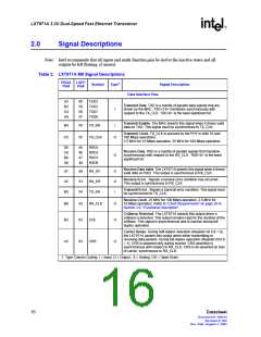
Table 3. LXT971A Network Interface Signal Descriptions
PBGA
Pin#
LQFP
Pin#
Symbol
Type1
Signal Description
Twisted-Pair/Fiber Outputs, Positive & Negative.
During 100BASE-TX or 10BASE-T operation, TPFOP/N pins drive
H2
H3
19
20
TPFOP
TPFON
O
802.3 compliant pulses onto the line.
During 100BASE-FX operation, TPFOP/N pins produce differential
LVPECL outputs for fiber transceivers.
Twisted-Pair/Fiber Inputs, Positive & Negative.
During 100BASE-TX or 10BASE-T operation, TPFIP/N pins receive
H4
H5
23
24
TPFIP
TPFIN
I
I
differential 100BASE-TX or 10BASE-T signals from the line.
During 100BASE-FX operation, TPFIP/N pins receive differential
LVPECL inputs from fiber transceivers.
Signal Detect2: Dual function input depending on the state of the
device.
Reset and Power-Up. Media mode selection:
Tie High for FX mode (Register bit 16.0 = 1)
Tie Low for TP mode (Register bit 16.0 = 0)
G2
26
SD/TP
Normal Operation (FX Mode): SD input from the fiber transceiver.
Normal Operation (TP Mode): Tie to GND (uses an internal pull-
down).
1. Type Column Coding: I = Input, O = Output, A = Analog, OD = Open Drain
2. For standard digital loopback testing (Register bit 0.14) in FX mode, the SD pin should be tied to an
LVPECL logic High (2.4 V).
Datasheet
17
Document #: 249414
Revision #: 002
Rev. Date: August 7, 2002

 INTEL [ INTEL ]