1-Gbit P30 Family
.
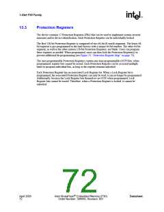
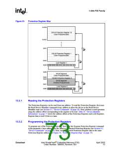
Figure 33.
Protection Register Map
0x109
128-bit Protection Register 16
(User-Programmable)
0x102
0x91
128-bit Protection Register 1
(User-Programmable)
0x8A
Lock Register 1
15 14 13 12 11 10
9
8
7
6
5
4
3
2
1
0
0x89
0x88
64-bit Segment
(User-Programmable)
0x85
0x84
128-Bit Protection Register 0
64-bit Segment
(Factory-Programmed)
0x81
0x80
Lock Register 0
15 14 13 12 11 10
9
8
7
6
5
4
3
2
1
0
13.3.1
Reading the Protection Registers
The Protection Registers can be read from any address. To read the Protection Register, first issue
the Read Device Identifier command at any address to place the device in the Read Device
Identifier state (see Section 9.2, “Device Commands” on page 50). Next, perform a read operation
using the address offset corresponding to the register to be read. Table 29, “Device Identifier
Information” on page 77 shows the address offsets of the Protection Registers and Lock Registers.
Register data is read 16 bits at a time.
13.3.2
Programming the Protection Registers
To program any of the Protection Registers, first issue the Program Protection Register command
at the parameter’s base address plus the offset to the desired Protection Register (see Section 9.2,
“Device Commands” on page 50). Next, write the desired Protection Register data to the same
Protection Register address (see Figure 33, “Protection Register Map” on page 73).
Datasheet
Intel StrataFlash® Embedded Memory (P30)
Order Number: 306666, Revision: 001
April 2005
73

 INTEL [ INTEL ]