Timing Model & Specifications
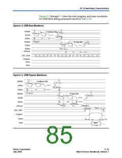
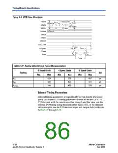
Figure 5–5. UFM Erase Waveforms
ARShft
9 Address Bits
tACLK
tAH
tASU
ARClk
ARDin
DRShft
DRClk
DRDin
DRDout
tADH
tADS
OSC_ENA
tOSCS
tOSCH
Program
Erase
tEB
tBE
Busy
tEPMX
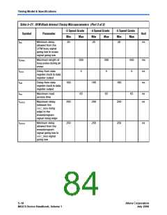
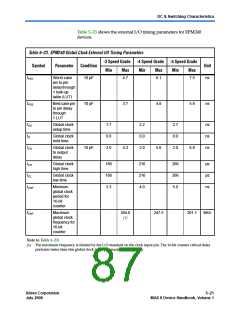
Table 5–22. Routing Delay Internal Timing Microparameters
-3 Speed Grade -4 Speed Grade
-5 Speed Grade
Routing
Unit
Min
Max
429
326
330
Min
Max
556
423
429
Min
Max
687
521
529
tC4
ps
ps
ps
tR4
tLOCAL
External Timing Parameters
External timing parameters are specified by device density and speed
grade. All external I/O timing parameters shown are for the 3.3-V LVTTL
I/O standard with the maximum drive strength and fast slew rate. For
external I/O timing using standards other than LVTTL or for different
drive strengths, use the I/O standard input and output delay adders in
Tables 5–27 through 5–31.
5–20
Core Version a.b.c variable
Altera Corporation
July 2006
MAX II Device Handbook, Volume 1

 INTEL [ INTEL ]