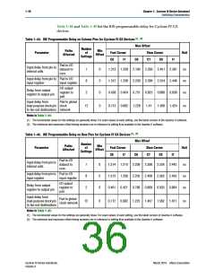
1–40
Chapter 1: Cyclone IV Device Datasheet
Glossary
Table 1–46. Glossary (Part 4 of 5)
Letter
Term
Definitions
tC
High-speed receiver and transmitter input and output clock period.
Channel-to-
channel-skew
(TCCS)
High-speed I/O block: The timing difference between the fastest and slowest output edges,
including tCO variation and clock skew. The clock is included in the TCCS measurement.
tcin
Delay from the clock pad to the I/O input register.
Delay from the clock pad to the I/O output.
tCO
tcout
tDUTY
tFALL
tH
Delay from the clock pad to the I/O output register.
High-speed I/O block: Duty cycle on high-speed transmitter output clock.
Signal high-to-low transition time (80–20%).
Input register hold time.
Timing Unit
Interval (TUI)
High-speed I/O block: The timing budget allowed for skew, propagation delays, and data
sampling window. (TUI = 1/(Receiver Input Clock Frequency Multiplication Factor) = tC/w).
tINJITTER
Period jitter on the PLL clock input.
tOUTJITTER_DEDCLK
tOUTJITTER_IO
tpllcin
Period jitter on the dedicated clock output driven by a PLL.
Period jitter on the general purpose I/O driven by a PLL.
Delay from the PLL inclk pad to the I/O input register.
Delay from the PLL inclk pad to the I/O output register.
tpllcout
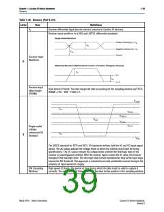
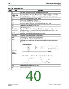
T
Transmitter output waveforms for the LVDS, mini-LVDS, PPDS and RSDS Differential I/O
Standards:
Single-Ended Waveform
Positive Channel (p) = VOH
VOD
Negative Channel (n) = VOL
V
os
Transmitter
Output
Ground
Waveform
Differential Waveform (Mathematical Function of Positive & Negative Channel)
VOD
0 V
VOD
p - n
tRISE
tSU
Signal low-to-high transition time (20–80%).
Input register setup time.
—
U
—
Cyclone IV Device Handbook,
Volume 3
March 2016 Altera Corporation

 INTEL [ INTEL ]