Host-PCI Express* Bridge Registers (D1:F0)
(Intel® 82915G/82915P/82915PL Only)
R
8.1.37
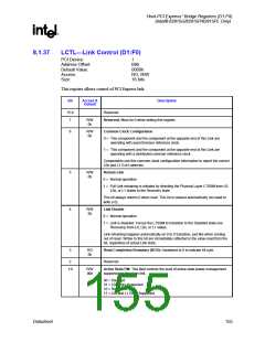
LCTL—Link Control (D1:F0)
PCI Device:
Address Offset:
Default Value:
Access:
1
B0h
0000h
RO, R/W
16 bits
Size:
This register allows control of PCI Express link.
Bit
Access &
Default
Description
15:8
7
Reserved
R/W
0h
Reserved. Must be 0 when writing this register.
6
R/W
0b
Common Clock Configuration
0 = This component and the component at the opposite end of this Link are
operating with asynchronous reference clock.
1 = This component and the component at the opposite end of this Link are
operating with a distributed common reference clock.
Components use this common clock configuration information to report the correct
L0s and L1 Exit Latencies.
5
R/W
0b
Retrain Link
0 = Normal operation
1 = Full Link retraining is initiated by directing the Physical Layer LTSSM from L0,
L0s, or L1 states to the Recovery state.
This bit always returns 0 when read. This bit is cleared automatically (no need to
write a 0).
4
R/W
0b
Link Disable
0 = Normal operation
1 = Link is disabled. Forces the LTSSM to transition to the Disabled state (via
Recovery) from L0, L0s, or L1 states.
Link retraining happens automatically on 0 to 0 transition, just like when coming
out of reset. Writes to this bit are immediately reflected in the value read from the
bit, regardless of actual Link state.
3
RO
0b
Read Completion Boundary (RCB): Hardwired to 0 to indicate 64 byte.
2
Reserved
1:0
R/W
00b
Active State PM: This field controls the level of active state power management
supported on the given link.
00 = Disabled
01 = L0s Entry Supported
10 = Reserved
11 = L0s and L1 Entry Supported
Datasheet
155

 INTEL [ INTEL ]