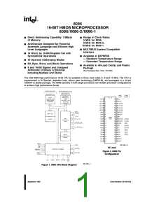
8086
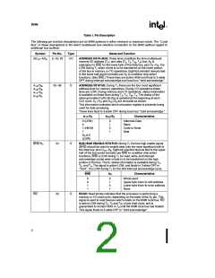
Table 1. Pin Description (Continued)
Name and Function
Symbol
Pin No.
Type
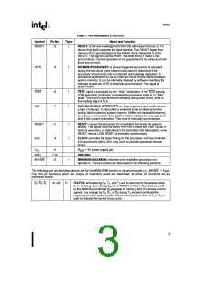
READY
22
I
READY: is the acknowledgement from the addressed memory or I/O
device that it will complete the data transfer. The READY signal from
memory/IO is synchronized by the 8284A Clock Generator to form
READY. This signal is active HIGH. The 8086 READY input is not
synchronized. Correct operation is not guaranteed if the setup and hold
times are not met.
INTR
18
I
INTERRUPT REQUEST: is a level triggered input which is sampled
during the last clock cycle of each instruction to determine if the
processor should enter into an interrupt acknowledge operation. A
subroutine is vectored to via an interrupt vector lookup table located in
system memory. It can be internally masked by software resetting the
interrupt enable bit. INTR is internally synchronized. This signal is
active HIGH.
TEST
NMI
23
17
I
I
TEST: input is examined by the ‘‘Wait’’ instruction. If the TEST input is
LOW execution continues, otherwise the processor waits in an ‘‘Idle’’
state. This input is synchronized internally during each clock cycle on
the leading edge of CLK.
NON-MASKABLE INTERRUPT: an edge triggered input which causes
a type 2 interrupt. A subroutine is vectored to via an interrupt vector
lookup table located in system memory. NMI is not maskable internally
by software. A transition from LOW to HIGH initiates the interrupt at the
end of the current instruction. This input is internally synchronized.
RESET
CLK
21
19
I
I
RESET: causes the processor to immediately terminate its present
activity. The signal must be active HIGH for at least four clock cycles. It
restarts execution, as described in the Instruction Set description, when
RESET returns LOW. RESET is internally synchronized.
CLOCK: provides the basic timing for the processor and bus controller.
It is asymmetric with a 33% duty cycle to provide optimized internal
timing.
a
5V power supply pin.
V
40
1, 20
33
V
CC
:
CC
GND
GROUND
MN/MX
I
MINIMUM/MAXIMUM: indicates what mode the processor is to
operate in. The two modes are discussed in the following sections.
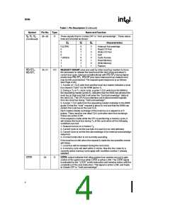
e
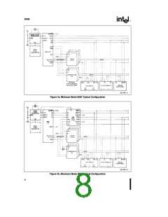
The following pin function descriptions are for the 8086/8288 system in maximum mode (i.e., MN/MX
V
).
SS
Only the pin functions which are unique to maximum mode are described; all other pin functions are as
described above.
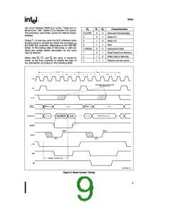
S , S , S
1
26–28
O
STATUS: active during T , T , and T and is returned to the passive state
4 1 2
(1, 1, 1) during T or during T when READY is HIGH. This status is used
2
0
3
W
by the 8288 Bus Controller to generate all memory and I/O access control
signals. Any change by S , S , or S during T is used to indicate the
beginning of a bus cycle, and the return to the passive state in T or T is
2
1
0
4
3
W
used to indicate the end of a bus cycle.
3

 INTEL [ INTEL ]